Page 47 - Chip Scale Review_November December_2022-digital
P. 47
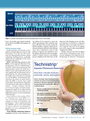
Figure 7: Schematic representation of a 3D-SoC with backside power delivery implementation.

        layers, electrically connecting the backside   few 100nm of Si is required to expose the   final step of the thinning process, the SiGe
        of the wafer to the BPR in the frontside via   nTSVs and minimize their resistivity (and   etch stop layer is removed in a dedicated
        the nTSVs.                         hence, IR drop). This severely restricts the   chemistry where very high selectivity to
                                           allowed thickness variation, which may be   Si is required. This way, the Si capping
        Critical process steps             induced during the different wafer thinning   layer can be exposed with a total thickness
          Implementing a backside power    steps. Imec collaborates with several   variation below 40nm.
        delivery network adds new steps to chip   partners to improve the chemistries used   Another concern is the thermal impact
        fabrication. Over the last few years,   for etching. The final wet etch, for example,   on the device self-heating because of the
        imec has demonstrated various critical   enables a highly selective soft-landing   extreme thinning of the (otherwise heat-
        technology building blocks, gradually   process stopping on the SiGe layer. In the   dissipating) Si substrate. Preliminary
        addressing the challenges of the novel
        production steps [3-5].
          BPR:  introducing  metal  in  the
        buried power rails are implemented in  Technistrip                ®
        FEOL. In the proposed fabrication flow,

        the FEOL, before device processing. This
        implementation means the metal rail is   Superior Photoresist Removers
        subject to the high-temperature process
        steps applied during subsequent device   More than a decade of industry
        manufacturing. For chip manufacturers,
        this might seem as disruptive as bringing   leadership, service, and support
        Cu into the BEOL several decades ago.
        Therefore, the choice of metal used to   Technic’s Technistrip  series of photoresist removal
                                                          ®
        make the BPR is crucial. Imec could   chemistries have grown to meet evolving demands of
        successfully demonstrate the integration   semiconductor fabricators, especially for wafer-level
        of buried power rails made of refractory   packaging applications including RDL, UBM, and
        metals – metallic elements like Ru   Cu pillar processing.
        or W that are highly resistant to heat.
        Keeping the metal rail en-capped during   •  Rapid and complete removal of a wide range
        subsequent FEOL processing was an        of photoresist materials
        additional measure to avoid contamination   •  High materials compatibility with metals
        of the front end.                        and compound semiconductor substrates
          Imec believes that using nTSVs
        i n c o m bi n a t io n w it h BPR s  i s  a   •  Best-in-class cost of ownership through
        ve r y p r om i si ng i mple me nt at ion   extended bath life, mild operating conditions,
        scheme in terms of scalability and       and straightforward rinsing
        performance. Other implementations    •  NMP - Free
        of a BSPDN exist as well, each trading
        off power deliver y perfor mance,
        standard cell area consumption and
        FEOL complexity.
          Wafer thinning: minimizing thickness
        variation. Extreme wafer thinning to a     www.technic.com

                                                                                                  6/15/2022   1:20:08 PM
                                             Chip Scale Review - Technistrip.indd   1             6/15/2022   1:20:08 PM
                                             Chip Scale Review - Technistrip.indd   1
                                                                                                             45
                                                       Chip Scale Review   November  •  December  •  2022   [ChipScaleReview.com]  45

