Page 36 - Chip Scale Review_November December_2022-digital
P. 36
Large-panel fan-out perspective on cost, yield,


        and capability

        By Clifford Sandstrom, Robin Davis, Benedict San Jose  [Deca Technologies, Inc.]

        W            i t h  s u pp l y  c ha i n   panel format will be described, including   panel format can fit 256 devices per panel,


                     shortages for many of
                                           mask-less laser direct imaging (LDI). Our
                     the traditional packaging   scaling to 2µm lines and spaces using   given the same 36mm x 36mm package area.
                                                                              This results in a format efficiency of 92%
        technologies, the semiconductor industry   patterning technology, a critical part of the   (see Figure 2b). The square panel format’s
        is looking for alternative solutions. One of   process, provides precise real-time design   nearly 20% higher utilization of molded area
        the key technologies under consideration   and alignment. This is critical in a multi-  translates directly to lower cost.
        by many is molded fan-out panel-level   die environment—providing the ability to   Figure 3a details the most highly utilized
        packaging (FOPLP). This technology is   implement high-density interconnects in a   materials in the process for M-Series 300mm
        particularly appealing as it offers a high-  large-panel format.      round wafer, shown as a percentage of
        density, high-throughput solution and can                             the total material cost. The polyimide and
        achieve comparable, or better, end results   Cost considerations      laminated films such as carrier laminate,
        as compared to conventional laminate or   To better explain the cost advantage of   temporary backside laminate (BSL) used for
        lead frame-based packages.         using a 600mm square large panel compared   warpage control, and photo dry film (DFR)
          Currently running at volumes in the   to the conventional 300mm round wafer,   represent more than 30% of the total bill of
        millions of units per day on a 300mm   an analysis of utilization and effective area   materials (BOM) cost. Consumption of these
        round format, Deca’s M-Series™ fan-out   is outlined using a concept called format   materials is directly proportional to the panel
                                        ®
        PLP technology and Adaptive Patterning    efficiency. To compute for the format   format efficiency described earlier. These
        have been scaled up to the new industry   efficiency of a fan-out molded panel, the total   materials correspond to potential cost savings
        standard 600mm x 600mm large-panel   usable package area is divided by the format   in a 600mm large-panel format by reducing
        format for production. The first 600mm   area. For example, let’s consider a 9-die   material wastage.
        production implementation in nepes   chiplet fan-out device with an overall package   An example of cost-saving opportunities
        laweh in Cheongan, South Korea, began   size of 36mm x 36mm molded in a 300mm   described above includes the following: using
        operations in 2021 and continues to ramp   round wafer. The 300mm wafer format   slot or slit coating is ideal for a square panel
                                                    2
        in production. The SEMI standard 600mm   (70,686mm ) can fit 40 packages per wafer   where just 22ml of polyimide is required for
        square format provides a 500% increase   (a total usable package area of 51,840mm )   a dielectric layer vs. the 8ml volume typically
                                                                           2
        in usable area per panel vs. 300mm round,   resulting in a format efficiency at 73% (see   used in spin coating on 300mm wafers. This
        providing cost-effective capacity growth   Figure 2a). In contrast, a 600mm large-  translates to a 44% reduction in volume
        as well as a powerful platform for high-
        density integration of multi-die and chiplets
        in 2D, 2.5D, and 3D structures.
          The 600mm square format was created
        with considerations for both short-term
        implementation and long-term optimized
        productivity. The ability to segment the
        600mm panels into four 300mm square
        sub-panels for use with conventional
        300mm round wafer probe test equipment
        was a driving factor for the short term
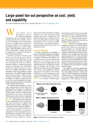
        (Figure 1).  Extending process capability
        for key lithography, metal deposition,
        and other processes to complete the
        600mm panel provided a challenging, yet
        achievable target for equipment suppliers.
          Focusing on economies of scale, the
        300mm round baseline is examined as
        compared to various large-panel formats.
        Implementation strategies of the industry’s
        first high-volume chips-first, chips-up
        M-Series fan-out structure in a large-  Figure 1: M-Series 300mm round and 600mm square panel.

        34   Chip Scale Review   November  •  December  •  2022   [ChipScaleReview.com]
        34

