Page 37 - Chip Scale Review_November December_2022-digital
P. 37
ability to scale to finer bond pad pitches, as
                                                                              further discussed below. This patterning
                                                                              technology includes the high-speed
                                                                              measurement of each die location within
                                                                              a panel, the creation of optimized unit-
                                                                              specific patterns for each device according
                                                                              to pre-determined design constraints, and
                                                                              the application of each layer of the design
                                                                              file through a maskless lithography system.
                                                                              Using this patterning technology, simple
                                                                              devices to complex heterogeneous multi-
                                                                              chiplet systems can be constructed cost-
                                                                              effectively with assurance of high yields in
                                                                              manufacturing.
                                                                                Multiple techniques are available to
                                                                              optimize the unit-specific pattern in
                                                                              response to die shift. The first, adaptive
                                                                              alignment, typically dynamically aligns the
                                                                              redistribution layer (RDL) and first via layer
                                                                              pattern to precisely match that of the die
                                                                              pads based on the measured lateral shift and
                                                                              rotation for each die. A further technique,
                                                                              adaptive routing, builds on top of adaptive
                                                                              alignment by regenerating small segments
                                                                              of RDL traces to maintain electrical
                                                                              connectivity between portions of the design
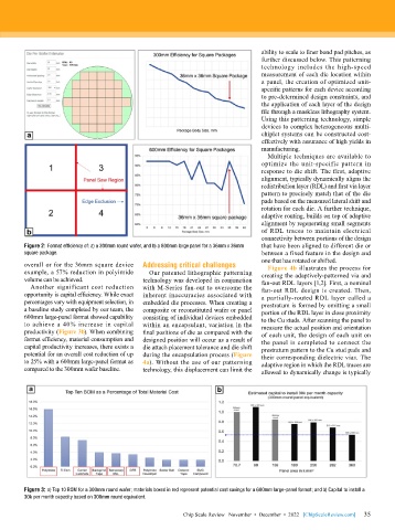
        Figure 2: Format efficiency of: a) a 300mm round wafer, and b) a 600mm large panel for a 36mm x 36mm   that have been aligned to different die or
        square package.                                                       between a fixed feature in the design and
                                                                              one that has rotated or shifted.
        overall or for the 36mm square device   Addressing critical challenges  Figure 4b illustrates the process for
        example, a 57% reduction in polyimide   Our patented lithographic patterning   creating the adaptively-patterned via and
        volume can be achieved.            technology was developed in conjunction   fan-out RDL layers [1,2]. First, a nominal
          Another significant cost reduction   with M-Series fan-out to overcome the   fan-out RDL design is created. Then,
        opportunity is capital efficiency. While exact   inherent inaccuracies associated with   a partially-routed RDL layer called a
        percentages vary with equipment selection, in   embedded die processes. When creating a   prestratum is formed by omitting a small
        a baseline study completed by our team, the   composite or reconstituted wafer or panel   portion of the RDL layer in close proximity
        600mm large-panel format showed capability   consisting of individual devices embedded   to the Cu studs. After scanning the panel to
        to achieve a 40% increase in capital   within an encapsulant, variation in the   measure the actual position and orientation
        productivity (Figure 3b). When combining   final positions of die as compared with the   of each unit, the design of each unit on
        format efficiency, material consumption and   designed position will occur as a result of   the panel is completed to connect the
        capital productivity increases, there exists a   die attach placement tolerance and die shift   prestratum pattern to the Cu stud pads and
        potential for an overall cost reduction of up   during the encapsulation process (Figure   their corresponding dielectric vias. The
        to 25% with a 600mm large-panel format as   4a). Without the use of our patterning   adaptive region in which the RDL traces are
        compared to the 300mm wafer baseline.  technology, this displacement can limit the   allowed to dynamically change is typically


        Figure 3: a) Top 10 BOM for a 300mm round wafer; materials boxed in red represent potential cost savings for a 600mm large-panel format; and b) Capital to install a
        30k per month capacity based on 300mm round equivalent.

                                                                                                             35
                                                       Chip Scale Review   November  •  December  •  2022   [ChipScaleReview.com]  35

