Page 25 - Chip Scale Review_November December_2022-digital
P. 25
In our study, FEA was used to investigate the risk for
        RDL cracking based on different trace dimensions and
        geometries such as trace width, trace thickness, trace length
        from via to turning point, and trace angle as shown in


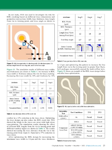
                                                             Table 4: Trace geometry effect on RDL crack risk.
        Figure 11: RDL trace geometry: A is the trace width, B is the trace space, C is   to 2.3µm and optimizing the pattern to increase the line
        the trace length from via to turning point, and D is the trace angle.
                                                             length from via to the turning point to greater than 18µm,
        Figure 11. The simulation results of different trace widths   both packages successfully passed the multi-reflow tests.
        and thicknesses are shown in Table 3. An increase in RDL   Figure 12 shows an example of the RDL trace design before
        trace width or thickness reduces the risk for trace cracking.   and after trace optimization.
        Increasing the trace width by 10% and thickness by 15%


                                                             Figure 12: RDL layout a) before and b) after trace optimization.


        Table 3: Line dimension effect on RDL crack risk.
        resulted in a 15% reduction in the trace stress. Optimizing
        the trace design can also reduce the RDL crack risk. FEA
        showed the bends in the traces are areas with high stress
        concentration. The simulation results showing the effect
        of different RDL lengths from the via to turning point and
        different teardrop angles are shown in Table 4. The results
        showed increasing the trace distance from the via to the
        turning point from 12µm to 18µm had a 57% reduction in
        trace stress.
          After optimizing the RDL design by increasing the
        minimum trace width to 2.2µm and the trace thickness
                                                             Table 5: Reliability test results.

                                                                                                             23
                                                       Chip Scale Review   November  •  December  •  2022   [ChipScaleReview.com]  23

