Page 30 - Chip Scale Review_November December_2022-digital
P. 30
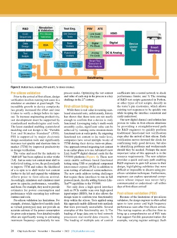
Figure 3: Multiple tools, including PSV and ATE, for device checkout.
        Pre-silicon validation             process nodes. Optimizing the test content   coefficients into a neural network to check
          Prior to the arrival of first silicon, design   and value of each step in the process is a key   performance limits; and 3) The running
                                                         st
        verification involves running test cases in a   challenge in the 21 century.   of R&D test scripts generated in Python,
        simulator or emulator at great length. The                            or other types of test scripts, directly in
        incredible growth in device complexity   First-silicon bring-up       the tester’s pin electronics, which allows
        has greatly increased the effort and time   While there is real value in running scan-  existing test sequences to be quickly run
        it takes to verify a design before its tape-  based structural tests, unfortunately, history   while keeping the interface consistent and
        out. To increase engineering productivity,   has shown that these tests are not nearly   easily understood.
        test development must be supported by   enough to confirm that a device is truly   Our new digital channel card solution has
        standardized methodologies and tools.   functional. Leveraging today’s multi-week   proven its value in first-silicon situations
        The latest standard enabling system-level   assembly cycles, significant value can be   by providing a straightforward path
        modeling and test design is the “Portable   achieved by running some mission-mode   for R&D engineers to quickly perform
        Test and Stimulus Standard” (PSS).   functional tests at wafer probe. By migrating   traditional functional test verification
        PSS is supported by major electronic   functional test content to the wafer level,   steps after the arrival of first silicon. Early
        design automation tools and significantly   companies have saved multiple weeks of   verification moves forward the clock for
        increases test quality and shortens time to   TTM during their device turn-on phase.   confirming truly good devices, but also
        market (TTM) by improved productivity   One approach toward migrating test content   to identifying problems and workarounds
        in design verification.            to an earlier phase is to use Advantest’s new   should they be needed. Perhaps the most
          The value and need for the industry to   Link Scale™ digital channel cards for the   important value of this approach is in the
        “shift left” has been explored in other works   V93000 platform (Figure 4). These new   resource requirements. The new solution
        [3,4].  Just as some test content must shift to   cards enable software-based functional   provides a quick and easy path enabling
        wafer-level testing, so too, the preferred path   testing using USB or peripheral component   R&D engineers to gain full access to their
        to improve TTM and reduce the likelihood   interconnect express (PCIe) in addition to   design, highlighting subtleties that were
        of a re-spin is to shift wafer test content   scan testing of advanced semiconductors.   difficult or impossible to discern using pre-
        further to the left and expand the validation   The new cards address testing challenges   silicon validation techniques. Furthermore,
        efforts prior to first-silicon arrival.   that require these interfaces to run in full   engineers can explore operational corner-
        Accordingly, simulators and emulators must   protocol mode, thereby adding System-Like-  cases whose impact was never fully
        grow in capacity, performance, versatility,   Test™ capabilities to the V93000.  communicated or understood—all within
        and focus. For example, they need to provide   Not only does a high-speed interface   days of first silicon arrival!
        estimates for power consumption and   such as PCIe enable scan over high-speed
        performance while executing key software   input/output (HSIO), but it also allows the   Post-silicon validation (PSV)
        routines and code.                 design team to confirm true functionality   Because of the limitations of pre-silicon
          Pre-silicon validation has limitations. For   deep within the silicon. Tests applied using   validation, the design engineer is often called
        example, abstract, higher-level models (such   this approach enable different tests methods   upon to tune power and high-frequency
        as virtual prototypes) may not provide an   that were previously unavailable. Several   performance soon after first silicon arrives.
        accurate estimate of the power consumption   examples of this functionality are: 1) The   This tuning requires an effective flow to
        for given code snippets. Even detailed models   loading of large data sets to feed network   bring up a comprehensive set of PSV tests
        often are significantly wrong in estimating   processors real-world data streams; 2)   that support flexible parameterization (for
        maximum frequency–-particularly for new   The loading of multiple sets of control   example, varying register settings). Such


        28   Chip Scale Review   November  •  December  •  2022   [ChipScaleReview.com]
        28

