Page 23 - Chip Scale Review_November December_2022-digital
P. 23
Table 1: Package attributes.                                            2
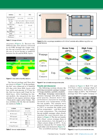
                                           Figure 3: a) Fan-out package assembled on a 91 X 91mm  substrate with a stiffener ring; b) Fan-out
        structure (Figure 2). Because the   module floor plan.
        different dies were directly connected
        to the RDL through the copper vias,
        the fan-out structure does not require
        the use of micro bumps or underfill
        between the die and the RDL layers.


        Figure 2: Cross section of an RDL structure.

          The fan-out package and floor plan   Figure 4: Fan-out module warpage contour plots.
        are shown in Figure 3. In the package,
        the SoC was connected to 8 identical   Results and discussion         is shown in Figure 6. Both TV1 and
        I/O dies with three RDL layers with   The following sections discuss the   TV2 had a convex warpage shape at
        line width and spacing of 2/2µm for   following assessments: package warpage,   room temperature, but turned to a
                                                                                                              2
        the first two layers and 5/5µm for the   C4 bump reliability, and RDL reliability.  concave shape at 250°C. The 91X91mm
        third layer. After building the fan-  Package warpage assessment.     package had 30% higher warpage at
        out module, the integrated die was   Because warpage will  affect  solder
        attached to an organic substrate using   joi nt qualit y, shadow moi ré was
        130µm pitch copper pillar bumps. The   performed to characterize warpage
        key attributes for the fan-out module   variations  over temperature  of the
        are shown in Table 2.              fan-out module. The samples were
                                           measured from room temperature up
                                           to 250°C to simulate the solder joint
                                           reflow temperature – and then down
                                           to room temperature. The simulated
                                           fan-out module warpage values closely
                                           matched the experimental data as
                                           shown in Figure 4. The fan-out module
                                           had a 69µm  convex warpage shape at
                                           room temperature, but changed to a
                                           -20µm concave shape at 250°C.  X-ray
                                           analysis showed the C4 bumps have
                                           good solder joint formation (Figure 5).
                                             The assembled package warpage
        Table 2: Fan-out module attributes.                                   Figure 5: X-ray of C4 joints near the die corner.

                                                                                                             21
                                                       Chip Scale Review   November  •  December  •  2022   [ChipScaleReview.com]  21

