Page 21 - Chip Scale Review_November December_2022-digital
P. 21
High-performance computing applications drive reli-


        ability of high-density fan-out packaging

        By Laurene Yip, Rosa Lin, Charles Lai, Cooper Peng  [MediaTek Inc.]

        T        he continuous drive for higher compute power   and high-performance applications. As the die size increases,


                 and greater data bandwidth to meet the growing
                                                             of thermal expansion (CTE) mismatch between the die and
                 demands from data centers, networking, and   the package stress also increases  because of the coefficient
        artificial intelligence (AI), has driven the development   the substrate and also increases the risk for package failures
        of advanced packaging solutions for higher performance   caused by bump cracks, mold compound delamination, and
        devices. Because single advanced node system on a chip   RDL failures in the fan-out package.
        (SoC) can no longer meet the increasing demands of high-  Our study assessed the reliability of large-format fan-out
        performance computing (HPC) applications, there is a   packages assembled with an application-specific integrated
        growing trend to use a chiplet architecture approach to split a   circuit (ASIC) die and  8 I/O chiplets using the chip-
        large, monolithic die into multiple smaller functional blocks,   first approach. The package robustness was investigated
        called chiplets, and reintegrating the chiplet dies using   using stringent component-level reliability testing, which
        advanced packaging. Chiplet architecture not only can bring   included temperature cycling (TC), an unbiased highly-
        the different functional blocks closer to each other to improve   accelerated temperature stress test (uHAST), and a high-
        device performance, but also can improve individual die   temperature storage (HTS) test.
        yields and help reduce the overall device cost [1-6].
          Among the advanced packaging technologies, wafer-  Package description
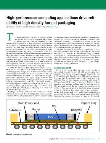
        level fan-out has emerged as an attractive package solution   In our study, multi-chip fan-out packages with an
        for heterogeneous integration. Wafer-level fan-out, which   integrated fan-out die size of 1.6X reticle size were
        uses fine-pitch redistribution layer (RDL) technology for   evaluated. The fan-out package integrated the ASIC die and
        die interconnection, can enable the development of high-  8 I/O chiplets with three layers of RDL interconnections.
        performance products with large package footprint, and   The fan-out die module was 41 X 33m m  and was
                                                                                                     2
        high interconnect density. Although silicon interposers had   assembled on low-loss organic substrates with sizes 74
        been widely used in the past for high-end server products,   X 74mm  and 91 X 91mm  as shown in  Figure 1. Both
                                                                     2
                                                                                    2
        silicon interposers that utilize through-silicon via (TSV)   packages used a copper stiffener ring for warpage control.
        technology have high manufacturing cost. Wafer-level   The key attributes of the test vehicles are summarized in
        fan-out with fine-pitch RDL is emerging as a lower cost   Table 1. The fan-out module was built using a process
        alternative package solution.                        where the different dies were attached to a temporary
          Package reliability, however, is becoming a critical   carrier and molded with epoxy mold compound to form a
        concern as the overall die size and package size increase to   reconstituted wafer. After molding, the multi-layer RDL
        accommodate the integration of more chiplets for networking   lines and C4 bumps were formed to create the fan-out die


        Figure 1: Cross section of a fan-out package.

                                                                                                             19
                                                       Chip Scale Review   November  •  December  •  2022   [ChipScaleReview.com]  19

