Page 16 - Chip Scale Review_November December_2022-digital
P. 16
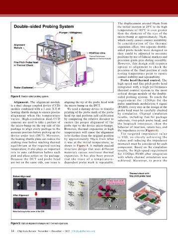
The displacement around 90μm from
                                                                              the initial location at 25ºC to the high
                                                                              temperature of 105ºC is even greater
                                                                              than the diameter of the size of the
                                                                              micro-bump at approximately 70µm,
                                                                              which easily causes contact instability.
                                                                              I n con side r at ion of t he t he r m al
                                                                              expansion effect, two separate double-
                                                                              sided probe heads were designed so
                                                                              they  could  be adjusted  to  accurate
                                                                              positions by use of fiducial markers and
                                                                              precision guide pins during assembly.
                                                                              However, this design still requires
                                                                              optical re-alignment to check the
                                                                              precision of the final position at each
                                                                              testing temperature point to ensure
                                                                              contact stability and repeatability.
                                                                                Probe head/thermal control. The
                                                                              high-speed and fine-pitch probe head
                                                                              integrated with a high-performance
                                                                              thermal  control system is the most
                                                                              critical design module of the double-
        Figure 4: Double-sided probing system.                                sided probing system. To reach the
                                                                              requirement for 112Gbps for the
          Alignment. The alignment module   aligning the tip of the probe head with   pulse amplitude modulation 4 signal
        is a dual-charge-coupled device (CCD)   the micro-bump on the DUT.    (PAM4), every step in the design of the
        module combined with a 3-axis X-Y-Θ   We used a dummy device to transfer   probe head must be carefully checked
        heating shuttle design to ensure precise   printing of the probe mark of the probe   by simulation. Channel simulation
        alig n ment when the temperat u re   head tip and perform self-calibration   results, including that for package
        varies. High-resolution dual-CCD   by computing the relative distance to   substrate, fine-pitch probe head, and
        cameras are used to take a picture of   ensure the proper alignment of the   the loopback interposer, show the
        the micro-bump on the top side of the   probe tips to the device micro-bumps.   behavior of insertion, return loss, and
        package to align every package to the   However, thermal expansion at high   the impedance curve (Figure 6).
        accurate position before picking up the   temperatures will cause the alignment   T he  t a rgeted  i mped a nce  value
        device under test (DUT). Moreover,   to be further from the original position   is  93Ω,  so  closely  achieving  the
        the heating shuttle plate can reduce the   by approximately 90µm from what   values and reducing the impedance
        soaking time before reaching thermal   it was at the initial temperature, as   mismatch must be considered for each
        equilibrium  at  the required  testing   shown in Figure 5. A multiple stacked   component. Based on the simulation
        temperature; it also plays an important   structure design that uses different   results, the high-speed requirement
        role in auto calibration before each   materials causes nonlinear thermal   for 112Gbps PAM4 after integration
        pick and place action on the package.   expansion. It has also been proven   with whole channel simulation was
        Because the DUT and probe head     that the t race of a temperat u re -  achieved. Moreover, to prove the
        are not on the same side, one issue is   dependent probe mark is repeatable.


        Figure 5: Optical alignment changes with thermal expansion.

        14
        14   Chip Scale Review   November  •  December  •  2022   [ChipScaleReview.com]

