
Page 13 - Chip Scale Review_November December_2022-digital
P. 13
Double-sided probing system for 150µm pitch
co-packaged optics
By Collins Sun [WinWay Technology]
T he focus of the double-sided Individual active and passive optical is predicted at around 55%, from US$6
probing system described
in this article is to be in components in a package can provide million in 2020 to US$2.2 billion by
the best performance and cost benefits
2032 [1].
alignment with trends in networking in a comprehensive manner. However, SiPh have been considered a unique
development. As expected, advanced more sophisticated processes in package tech nolog y for developing high-
packaging technology will continue to assembly also mean that it is critical to per for ma nce net work i ng system
extend Moore’s Law, particularly the have the assured yield after assembling because of several factors. First, it can
rapid development of heterogeneous all the discrete chips. Co-packaged be designed and manufactured using
integration (HI). According to various optics (CPO) is one representative current complementary metal-oxide
organizations, such as IEEE, SEMI, application—its optical signal has semiconductor (CMOS) processes and
and ASME, the essential spirit of HI a better signal-to-noise ratio than equipment, thereby achieving lower
is to integrate different process nodes electrical signals because of the light cost and higher performance devices.
and application-specific integrated being transmitted through an optic fiber Second, it can be combined with logic
circuits (ICs) into a single high- rather than electrical signals through and digital circuits for data processing.
end package, such as a 3D structure a copper trace. Having optical engines Third, SiPh can be designed using
system-in-package (3D SiP). When near the electrical switch to reduce different wafer materials, such as III-V
HI is combined with silicon photonics signal trace length in the substrate compound semiconductors. The future
(SiPh), trace loss from pluggable by advanced package technology is a of SiPh will flow into two main streams:
optics is greatly reduced and is able breakthrough technology. According to co-packaging and chip integration. Co-
to drive higher performance Ethernet Yole Intelligence, the compound annual packaging is the 2.5D integration of the
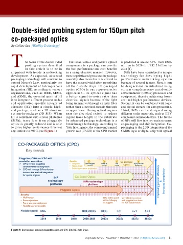
applications to 800G (see Figure 1). growth rate (CAGR) of the CPO market CMOS logic or digital chip with optical
Figure 1: Development trends in pluggable optics and CPO. SOURCE: Yole Group
Chip Scale Review November • December • 2022 [ChipScaleReview.com] 11 11