
Page 15 - Chip Scale Review_November December_2022-digital
P. 15
chips connected by the copper trace of
substrate. Chip integration is a single
complete chip solution that includes
different functional ICs using through-
silicon vias (TSVs) both for ASICs
and optical die. SiPh are expected to
integrate all optical components, such
as filter, polarization diversity, and
splitter/combiner into a single die,
including an active laser, modulator,
and photodetector. With the help of
SiPh and photonic integrated circuits
(PICs), CPO applications will be more
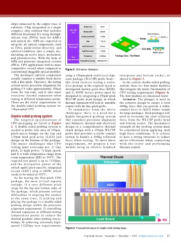
competitive overall when compared to Figure 2: CPO device information.
conventional pluggable optical modules.
The packaged optical component using a 150µm-pitch wafer-level chip- inter poser and bottom socket, as
usually requires a smaller form factor scale package (WLCSP) probe head— shown in Figure 3.
with a fine pitch. Therefore, the testing this trend involves testing a wafer- In the current double-sided probing
system needs precision alignment for level package at the required speed to system, there are four major modules
probing C4 sides approximately 150µm distinguish known good dies (KGD); that integrate the whole functionality of
from the top side, and it also must and 5) 600W device power must be CPO testing requirements (Figure 4).
overcome thermal expansion when dissipated by integrating a 150µm-pitch The four modules are discussed below.
testing at different temperature points. WLCSP probe head design, in which Actuator. The plunger is used in
These are the initial requirements for thermal expansion will lead to unstable the actuator design to ensure a total
the double-sided probing system for contact with the fine-pitch probe. 600kg force that can provide a stable
150µm-pitch CPO. To su m ma r i ze f rom t he above contact force to fulfill future trends
challenges: there is a need for a for large packages. Such packages will
Double-sided probing system highly-integrated probing system need to overcome the total reflected
T he t argeted specif ications of that considers precision alignment force from the WLCSP probe head
CPO packaging are listed in Figure and balances thermal and electrical and bottom socket. The mechanical
2. A double-sided probing system is design in a comprehensive thermal strength of the probing system must
needed to probe four sites of 150µm- chuck design with a 150µm WLCSP be considered when applying such
pitch micro-bumps on the top and probe that provides a stable contact high force conditions. It is critical
1.0mm land grid array (LGA) pad system to handle a 100kg ref lected to have a strong structure to reduce
design on the bottom of the package. force when testing. To meet these micro-vibrations when connecting
T he m ajor ch a l le nge s t h at C PO requi rements, we propose a test w it h t he t e s t e r a nd p e r fo r m i ng
testing must overcome are: 1) fine module using an electric loopback thermal control.
pitch, 2) high power, 3) high speed,
and 4) a wide temperature range from
room temperature (RT) to 105ºC. The
required test speed is up to 112Gbps,
and the dissipation power of the
switch application-specific integrated
circuit (ASIC) chip is 600W, which
needs to be tested at 105ºC.
As for testing the fine-pitch CPO
package, the most critical aspects
include: 1) a ver y different pitch
range for the top and bottom sides of
the package, which presents serious
difficulties in aligning the contact
at the same time; 2) picking and
placing the package in a double-sided
probing design within the precision
alignment requirement; 3) controlling
thermal expansion at different testing
temperature points to reduce the
thermal gradient when probing micro-
bumps; 4) achieving extremely high-
speed 112Gbps test requirements
Figure 3: Proposed test module for double-sided probing design.
13
Chip Scale Review November • December • 2022 [ChipScaleReview.com] 13