Page 24 - Chip Scale Review_November December_2022-digital
P. 24
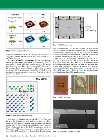
Figure 8: D2D RDL routing areas.
                                                             high stress due to the low CTE and high modulus of the silicon
        Figure 6: Package warpage contour plots.             die constraining the thermal expansion and shrinkage of the
                                                             copper lines [7]. The smaller the gap, the more the RDL line is
                                       2
        room temperature than the 74X74 mm  package. At 250°C, the   constrained by the silicon die and the higher the stress in the
                2
        91X91mm  package warpage was 60% higher compared to the   copper line, which increases the RDL trace crack risk.
                2
        74X74mm  package.                                      After TV1 and TV2 underwent multi-reflow testing at 250°C,
          C4 bump reliability assessment. Temperature cycling   package failures were observed to have trace cracking in the
        accelerates the thermo-mechanical failures caused by CTE   RDL lines. The trace cracks were typically observed in the
        mismatch. C4 bump joint crack risk increases as the fan-out   RDL2 lines underneath the main SoC near the die edge. The
        module size increases. Finite element analysis (FEA) showed the   trace cracks were mainly found on the isolated lines near the
        bumps at the die corner experience the highest stress and are at   tear drop turning point as shown in Figure 9. A cross section
        the greatest risk for cracking as shown in Figure 7. Both fan-out   of the RDL trace crack is shown in Figure 10. No trace cracks
        package test vehicles passed temperature cycling testing without   were found in the dense RDL metal line areas.
        any C4 bump failures.


                                                             Figure 9: An RDL trace crack.


        Figure 7: Copper pillar bump at the die corner.
          RDL trace reliability assessment. The CTE differences
        between the dielectric materials and copper lines in the RDL
        structure cause copper/dielectric interface distortion during
        temperature cycling that can result in RDL trace cracking.
        Figure 8 shows the die-to-die (D2D) routing areas where the
        high-density RDL lines interconnect the dies. Stress analysis
        showed the RDL traces between the gap of the dies experience   Figure 10: Cross section of the RDL trace crack.

        22
        22   Chip Scale Review   November  •  December  •  2022   [ChipScaleReview.com]

