Page 23 - Chip Scale Review_January February_2022-digital
P. 23
Bridges for chiplet design and heterogeneous


        integration packaging


        By John H. Lau  [Unimicron Technology Corporation]
        T        here are many advanced


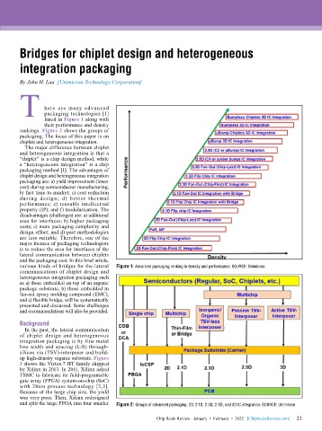
                 packaging technologies [1]
                 listed in Figure 1 along with
                 their performance and density
        rankings. Figure 2 shows the groups of
        packaging. The focus of this paper is on
        chiplets and heterogeneous integration.
          The major difference between chiplet
        and heterogeneous integration is that a
        “chiplet” is a chip design method, while
        a “heterogeneous integration” is a chip
        packaging method [1]. The advantages of
        chiplet design and heterogeneous integration
        packaging are: a) yield improvement (lower
        cost) during semiconductor manufacturing;
        b) fast time-to-market; c) cost reduction
        dur ing desig n; d) bet ter ther mal
        performance; e) reusable intellectual
        property (IP); and f) modularization. The
        disadvantages (challenges) are: a) additional
        area for interfaces; b) higher packaging
        costs; c) more packaging complexity and
        design effort; and d) past methodologies
        are less suitable. Therefore, one of the
        major focuses of packaging technologists
        is to reduce the area for interfaces of the
        lateral communication between chiplets
        and the packaging cost. In this brief article,
        various kinds of bridges for the lateral   Figure 1: Advanced packaging ranking in density and performance. SOURCE: Unimicron
        communications of chiplet design and
        heterogeneous integration packaging such
        as a) those embedded on top of an organic
        package substrate, b) those embedded in
        fan-out epoxy molding compound (EMC),
        and c) flexible bridge, will be systematically
        presented and discussed. Some challenges
        and recommendations will also be provided.

        Background
          In the past, the lateral communication
        of chiplet design and heterogeneous
        integration packaging is by fine metal
        line width and spacing (L/S) through-
        silicon via (TSV)-interposer and build-
        up high-density organic substrate. Figure
        3 shows the Virtex-7 HT family shipped
        by Xilinx in 2013. In 2011, Xilinx asked
        TSMC to fabricate its field-programable
        gate array (FPGA) system-on-chip (SoC)
        with 28nm process technology [2,3].
        Because of the large chip size, the yield
        was very poor. Then, Xilinx redesigned
        and split the large FPGA into four smaller   Figure 2: Groups of advanced packaging: 2D, 2.1D, 2.3D, 2.5D, and 3D IC integration. SOURCE: Unimicron

                                                                                                             21
                                                          Chip Scale Review   January  •  February  •  2022   [ChipScaleReview.com]  21

