Page 18 - Chip Scale Review_January February_2022-digital
P. 18
3D interconnect inspection for heterogeneous chip


        packaging using WSI


        By Shahab Chitchian  [INTEKPLUS CO., LTD.]
        H          eterogeneous integration


                   through the use of chiplet
                   pa ck ag i n g ,  i n clud i ng
        f a n - ou t  wa fe r-le vel p a ck a g i ng
        (WLP) and panel-level packaging
        (PLP) architecture, has become a key
        technology to continue Moore’s Law
        by improving yield and reducing total
        product cost [1,2]. Another important
        driver for heterogeneous integration
        is to improve performance and power
        efficiency, which can be achieved
        by decreasing interconnect pitch
        and increasing interconnect density.
        Therefore, capable 3D interconnect/
        bump inspection is necessary to enable
        heterogeneous packaging.
          In this article, white-light scanning
        interferometry (WSI) technology  is
        presented for the latest heterogeneous
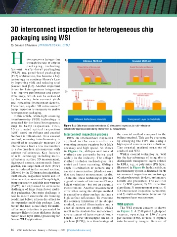
        chip 3D bu mp i nspect ion. Fi rst,   Figure 1: a) Oblique and coaxial methods for 3D interconnect inspection; b) multi-reflectance
        3D  automated  optical  inspection   detection for layer separation during interconnect 3D measurement.
        (AOI) based on oblique and coaxial                                    the coaxial method compared to the
        methods is introduced. As a coaxial   Interconnect inspection process  oblique method. This can be overcome
        method, scanning interferometry is   100% 3D interconnect inspection   by enlarging the FOV and using a
        described to accurately measure 3D   a p p l i e d  i n  t h e  s e m i c o nd u c t o r   high-speed camera as two solutions.
        interconnects from a few micrometers   mounting process requires both high   T he coa x ial met ho d con sist s of
        to a few hundred micrometers  with   accuracy and high speed. As shown   confocal and WSI.
        various ref lectances. Key features   in  Figure 1a, oblique and coaxial   Within coaxial technologies, WSI
        of WSI technology including multi-  methods are currently being used   has the key advantage of being able to
        reflectance surface 3D measurement,   widely in the industry. The oblique   distinguish transparent layers related
        high-speed camera, custom-made frame   method includes technologies like   to RDLs, e.g., a polyimide (PI) layer,
        grabber, and large field of view (FOV)   moiré and laser scanning. Oblique   illustrated in Figure 1b. In this article, an
        are introduced in the second section,   angle illumination or camera angle   interferometry system is discussed for 3D
        followed by the 3D inspection algorithm.   causes a nonsensitive (shadow) zone   interconnect inspection and metrology
        Furthermore, inspection results and 3D   that may impact measurement results.   of microelectronic devices; preliminary
        interconnect parameters of bump height,   Therefore, these technologies provide   results are presented. The outlines
        bump coplanarity, and chip area warpage   a good estimate of interconnect/bump   are: 1) WSI system; 2) 3D inspection
        (CAW) are explained to overcome    height variation—but not an accurate   algorithm; 3) measurement results; 4)
        challenges of large form factor multi-  measurement. Another measurement   3D interconnect inspection parameters;
        chip packaging. One main challenge is   error when using the oblique method   and 5) multi-reflectance detection for
        how to assure successful die bonding   is caused by a shiny surface that has a   transparent layer measurement.
        conditions before silicon die attach to   high surface reflectance. To overcome
        the expensive multi-chip package. Last,   the accuracy limitation of the oblique
        but not the least, a case study for multi-  method, coaxial illumination and a   WSI system
        reflectance detection is presented to   coaxial camera are applied, which   The WSI system concept is shown
        measure dielectric layer thickness during   result in the shadow-free and accurate   in Figure 2. A 25M pixel high-speed
        redistributed layer (RDL) processing for   measurement of interconnect/bump   camera, operating at 150 f rames
        fan-out WLP applications.          height. Lower throughput (in units   per second (FPS), is used to capture
                                           per hour [UPH]), is a disadvantage of   interferometry images. Because of

        16   Chip Scale Review   January  •  February  •  2022   [ChipScaleReview.com]
        16

