Page 20 - Chip Scale Review_January February_2022-digital
P. 20
3D inspection algorithm
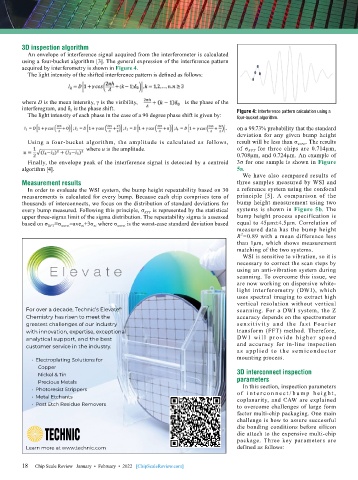
          An envelope of interference signal acquired from the interferometer is calculated
        using a four-bucket algorithm [3]. The general expression of the interference pattern
        acquired by interferometry is shown in Figure 4.
          The light intensity of the shifted interference pattern is defined as follows:


        where D is the mean intensity, γ is the visibility,    is the phase of the
        interferogram, and δ 0  is the phase shift.
          The light intensity of each phase in the case of a 90 degree phase shift is given by:  Figure 4: Interference pattern calculation using a
                                                                              four-bucket algorithm.
                                                                              on a 99.73% probability that the standard
                                                                              deviation for any given bump height
          Using a four-bucket algorithm, the amplitude is calculated as follows,   result will be less than σ worst . The results
                              where u is the amplitude.                       of  σ RPT  for three chips are 0.714μm,
                                                                              0.708μm, and 0.724μm. An example of
          Finally, the envelope peak of the interference signal is detected by a centroid   3σ for one sample is shown in Figure
        algorithm [4].                                                        5a.
                                                                                We have also compared results of
        Measurement results                                                   three samples measured by WSI and
          In order to evaluate the WSI system, the bump height repeatability based on 30     a reference system using the confocal
        measurements is calculated for every bump. Because each chip comprises tens of   principle [5]. A comparison of the
        thousands of interconnects, we focus on the distribution of standard deviations for   bump height measurement using two
        every bump measured. Following this principle, σ RPT  is represented by the statistical   systems is shown in Figure 5b. The
        upper three-sigma limit of the sigma distribution. The repeatability sigma is assessed   bump height process specification is
        based on σ RPT ≡σ worst =ave σi +3σ σi  where σ worst  is the worst-case standard deviation based   equal to 45μm±4.5μm. Correlation of
                                                                              measured data has the bump height
                                                                                2
                                                                              R =0.89 with a mean difference less
                                                                              than 1μm, which shows measurement
                                                                              matching of the two systems.
                                                                                WSI is sensitive to vibration, so it is
                                                                              necessary to correct the scan steps by
                                                                              using an anti-vibration system during
                                                                              scanning. To overcome this issue, we
                                                                              are now working on dispersive white-
                                                                              light interferometry (DWI), which
                                                                              uses spectral imaging to extract high
                                                                              vertical resolution without vertical
          For over a decade, Technic’s Elevate                                scanning. For a DWI system, the Z
                                        ®
          Chemistry has risen to meet the                                     accuracy depends on the spectrometer
          greatest challenges of our industry                                 se n sit iv it y a nd t he fa st Fou r ie r
          with innovation, expertise, exceptional                             transform (FFT) method. Therefore,
          analytical support, and the best                                    DW I w i l l p r ov id e h ig he r s p e e d
          customer service in the industry.                                   and accuracy for in-line inspection
                                                                              as applied to the sem iconductor
           •  Electroplating Solutions for                                    mounting process.
                Copper
                Nickel & Tin                                                  3D interconnect inspection
                Precious Metals                                               parameters
                                                                                In this section, inspection parameters
           •  Photoresist Strippers                                           o f i n t e r c o n n e c t / bu m p h e i g h t ,
           •  Metal Etchants                                                  coplanarity, and CAW are explained
           •  Post Etch Residue Removers                                      to overcome challenges of large form
                                                                              factor multi-chip packaging. One main
                                                                              challenge is how to assure successful
                                                                              die bonding conditions before silicon
                                                                              die attach to the expensive multi-chip
                                                                              package. Three key parameters are
          Learn more at www.technic.com                                       defined as follows:

                                                             1/19/2022   10:41:44 AM
          Chip Scale Review - Jan-Feb 2022.indd   1
          Chip Scale Review - Jan-Feb 2022.indd   1          1/19/2022   10:41:44 AM
        18   Chip Scale Review   January  •  February  •  2022   [ChipScaleReview.com]
        18

