Page 19 - Chip Scale Review_January February_2022-digital
P. 19
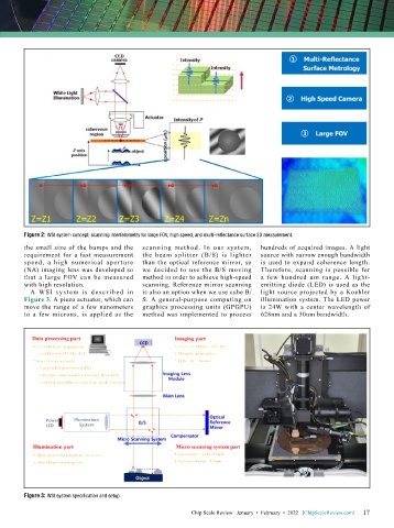
Figure 2: WSI system concept: scanning interferometry for large FOV, high speed, and multi-reflectance surface 3D measurement.
        the small size of the bumps and the   scanning method. In our system,   hundreds of acquired images. A light
        requirement for a fast measurement   the beam splitter (B/S) is lighter   source with narrow enough bandwidth
        speed, a high numerical aperture   than the optical reference mirror, so   is used to expand coherence length.
        (NA) imaging lens was developed so   we decided  to use the B/S  moving   Therefore, scanning is possible for
        that a large FOV can be measured   method in order to achieve high-speed   a few hundred um range. A light-
        with high resolution.              scanning. Reference mirror scanning   emitting diode (LED) is used as the
          A  WSI  system is descr ibed  i n   is also an option when we use cube B/  light  source  projected  by  a  Koehler
        Figure 3. A piezo actuator, which can   S. A general-purpose computing on   illumination system. The LED power
        move the range of a few nanometers   graphics processing units (GPGPU)   is 24W with a center wavelength of
        to a few microns, is applied as the   method was implemented to process   628nm and a 30nm bandwidth.


        Figure 3: WSI system specification and setup.

                                                                                                             17
                                                          Chip Scale Review   January  •  February  •  2022   [ChipScaleReview.com]  17

