Page 14 - Chip Scale Review_January February_2022-digital
P. 14
rates during the production process. The
        main purpose of this project is to widen
        the range of available miniaturization and
        microelectronic fabrication possibilities,
        including novel approaches in assembly
        processes added directly into production
        steps. TINKER will also train PhD and
        MSc students and aim to publish scientific
        papers and protect intellectual property.
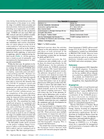
          The TINKER consortium comprises
        10 companies, three research specialists,
        one consultancy and a service association,
        who are major players in the field of   Table 1: The TINKER consortium.
        semiconductor  and  microelectronic
        manufacturing, as well as in the fields of   high-level overview about the activities   Grant Agreement nº 958472 with an overall
        material and process development and   centered on the pick-and-place equipment   budget of € 10,241,526.25. The project is
        industrial fields applying, or interested   and shows an early prototype of the   coordinated by scientist Leo Schranzhofer
        in applying, additive manufacturing for   RADAR demonstrator. It also touches on   at PROFACTOR GmbH. Discover more
        their needs (Table 1). All the partners   the metrology systems that are developed   about the project on its website (www.
        have a track record of nationally- and   by BESI and SENTECH.         project-tinker.eu) and on its social media
        internationally-funded projects in their   Another report presents the NIL   platforms linkedin.com/in/tinker-eu-
        special research fields.           infrastructure and available tools, as well   ba27b01b9 and twitter.com/project_tinker.
          Within the first year, the partners in the   as those developed specifically for the
        consortium have made significant progress   TINKER project. For the realization of   Reference
        in creating the proposed TINKER pilot   LiDAR sensors, the TINKER consortium   1.  Yole Développement (2021, September
        line and the innovative techniques it aims   is developing a NIL-based fabrication   2). LiDAR adoption: Technology
        to employ, especially pick and place,   method for photonic integrated circuits.   choices and supply chain management
        inkjet printing and NIL. Partners are   The photonic integrated circuit is the   are the key enablers [Press release].
        working on developing and perfecting   very precise core element necessary for   www.yole.fr/iso_upload/News/2021/
        designs, processes and materials required   the manipulation of light for each LiDAR   PR_LIDAR_AUTOMOTIVE and
        for the two selected use cases. They have   sensor. The aim of TINKER is to replace   INDUSTRIAL_MarketUpdate_
        been able to overcome the obstacles that   certain fabrication steps in an optical   DesignWins_Yole_September2021.pdf
        the COVID-19 pandemic posed and    phased array (OPA) process flow with NIL
        collaborated successfully on developing   in order to achieve fast and reliable direct   Biographies
        equipment and tools and shared samples,   manufacturing of the needed passive   Leo Schranzhofer is Lead Scientist and
        technologies, and processes. Examples   optical elements, such as the waveguides   Head of the “Functional Surfaces and
        of such fruitful collaborations are   and optical coupling structures. This   Nanostructures” team at PROFACTOR
        the completion of the pick-and-place   will reduce the size of the photonic IC   GmbH in Steyr, Austria and project
        equipment prototype, creation of the initial   device and its fabrication costs, as well as   coordinator of the TINKER project.
        setup for improved inline monitoring and   increase the throughput of its production.   He has a doctorate in chemistr y,
        feedback, and the infrastructure and tools   With the completion of this deliverable, the   specialized in analytical chemistry and
        set up for NIL. The consortium has made   TINKER consortium has now completed   chemical sensors, from the U. of Vienna.
        significant progress in equipment and   the equipment and tools development for   Email: leo.schranzhofer@profactor.at
        tools development for the TINKER pilot   the use case in TINKER.        Martin Eibelhuber is Deputy Head
        line, and a solid base for achieving the   An important goal is to integrate inline   of Bu si ness Development at EV
        project’s ambitious goals is now created.   process monitoring for different production   Group, Austria, focusing on compound
        One year after the project’s launch, it is   processes: pick and place, inkjet printing,   semiconductors, nanotechnology,
        well on track to reach its aim of widening   and NIL. These processes pose multiple   and photonics applications. He has a
        the range of available miniaturization and   requirements on inspection and inline   doctorate in Technical Physics from the
        microelectronic fabrication possibilities,   monitoring. Sensor technology deployed   Johannes Kepler U. Linz, specializing in
        and introducing novel approaches to   in TINKER to meet these requirements   nanoscience and semiconductor physics.
        assembly processes, directly in production.  comprise optical inspection, curing sensor,   Martina Chopart, MSc., is an EU Project
          The first public results can be accessed   and thermographic imaging. This is   Manager at AMIRES s.r.o. in Prague,
        via the project webpage (https://www.  covered in the third report.   where she is responsible for management
        project-tinker.eu/downloads/#public_  This project has received funding from   and dissemination of projects within the
        deliverables) and are summarized in   the European Union’s Horizon 2020   DeepTech program.
        three reports. The first report provides a   research and innovation program under the

        12
        12   Chip Scale Review   January  •  February  •  2022   [ChipScaleReview.com]

