Page 27 - Chip Scale Review_January February_2022-digital
P. 27
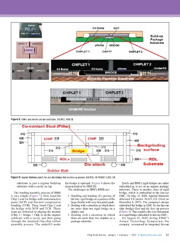
Figure 8: IBM’s test vehicle and demonstration. SOURCE: IBM [9]


        Figure 9: Applied Materials patent: fan-out chip (bridge) first and face-up process. SOURCE: US PATENT 10,651,126
            substrate is just a regular build-up   the bridge is optional. Figure 8 shows the   Intel’s and IBM’s rigid bridges are either
            substrate with a cavity on top.  demonstration by IBM [9].        embedded in, or are on an organic package
                                             The challenges in IBM’s DBHi are:  substrate. There is another class of rigid
          The bonding assembly process of DBHi                                bridge, which is embedded in the fan-out
        is very simple (Figure 7). First, bond the   1.  Handling and bonding of a portion of   EMC. On May 12, 2020, Applied Materials
        Chip 1 and the bridge with nonconductive   the tiny rigid bridge on a portion of the   obtained US patent 10,651,126 (filed on
        paste (NCP) and thermal compression    large chiplet with very fine-pitch pads;   December 8, 2017). The company’s design
        bonding (TCB). Then, bond Chip 2 and   2. Dealing with a situation in which there   embedded the bridge in EMC by the fan-out
        the bridge with NCP and TCB. Those     are more than one rigid bridge on a   chip (bridge) first and die face-up process
        steps are followed by placing the module   chiplet; and               (Figure 9). This could be the very first patent
        (Chip 1 + bridge + Chip 2) on the organic   3.  Dealing with a situation in which   of a rigid bridge embedded in fan-out EMC.
        substrate with a cavity and then going   there are more than two chiplets on a   On August 25, 2020, during TSMC’s
        through the standard flip-chip reflow   package substrate.            Annual Technology Symposium, the
        assembly process. The underfill under                                 company  announced its integrated fan-out


                                                                                                             25
                                                          Chip Scale Review   January  •  February  •  2022   [ChipScaleReview.com]  25

