Page 32 - Chip Scale Review_January February_2022-digital
P. 32
Managing trade-offs in the chiplet era


        By Rob Munoz  [Intel]

        I     n his famous 1965 paper [1]


              Gordon Moore foreshadowed that
              a chiplet-like approach would
        become attractive. By chiplets, we mean
        die that have been optimized to connect
        to other die within the same packaged
        device. Intel has used the term “tiles”
        to describe chiplets that are integrated
        using  high-density,  high-bandwidth
        interconnects enabled by advanced
        packaging technologies such as Intel’s
        2.5D embedded multi-die interconnect
        bridge (EMIB) [2], 3D Foveros [3], and
        combined EMIB-Foveros (Co-EMIB)
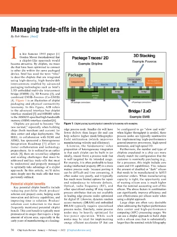
        [4]. Figure 1 is an illustration of chiplet
        packaging and physical connectivity
        taxonomy. In this figure, AIB refers
        to the advanced interface bus chiplet
        interface standard [5] and HBMIO refers
        to the JESD235-specified high-bandwidth
        memory (HBM) interface standard [6].
          Chiplets are poised to become “the   Figure 1: Chiplet packaging and physical connectivity taxonomy with examples.
        new normal,” especially when building
        chips (both merchant and custom) for   edge process node. Smaller die will have   be configured to go “slow and wide”
        data center and edge deployments. The   fewer defects than larger die and can   when higher throughput is needed, these
        IEEE, in collaboration with SEMI and   help achieve higher mask/lithographic   process nodes are typically unattractive
        ASME, has sponsored a Heterogeneous   f ield utilization (which improves   for implementing high-performance
        Integration Roadmap [7] effort to   manufacturing velocity and efficiency).  general-purpose processors, high-speed
        foster collaboration and technology   Likewise, the fundamental value   memories, and high-speed I/O.
        preparedness. As is outlined in an earlier   proposition of heterogeneous integration   Furthermore, the number and type of
        article [8], there are several key adoption   is that each chiplet can be built in (or   chiplets populated in a chip can more
        and scaling challenges that must be   ideally, reused from) a process node that   closely match the configuration that the
        addressed and key trade-offs that must   is well targeted for its intended usage.   customer is nominally purchasing (e.g.,
        be understood and properly managed   For example, it is often preferable to keep   for a processor, this might include core
        to optimally take advantage of a chiplet   analog intellectual property (IP) in a more   count and I/O capabilities). This reduces
        approach. In this article, we’ll delve   mature process node  because porting it   the amount of disabled or “dark” silicon
        more deeply into the trade-offs that were   can be difficult and time consuming, it   that needs to be manufactured to fulfill
        previously outlined.               often scales very poorly, and it typically   customer orders. When manufacturing
                                           has much more limited options for repair   capacity is tight, the opportunity cost
        Potential chiplet benefits         and redundancy to tolerate defects.   of wasting silicon area is much higher
          Key potential chiplet benefits include   Optical, radio frequency (RF), and   than the nominal accounting cost of this
        reducing portfolio (both product/  other specialized analog IP may require   silicon. The above factors in combination
        solution and project) costs, helping scale   process attributes that are not available   can significantly improve efficiency and
        innovation and delivery capabilities, and   in leading edge process nodes optimized   cost effectiveness per silicon wafer when
        improving time to solution. Product/  for digital IP. Likewise, dynamic random   using a chiplet approach.
        solution cost reduction is the most   access memory (DRAM) and embedded   Large chips are often very desirable
        frequently mentioned potential chiplet   DRAM typically require specialized   when addressing the highest performance
        benefit. This cost benefit is typically most   process nodes. Similarly, some process   data  center  and  high-performance
        pronounced in usages that require a large   nodes may be heavily optimized for   computing (HPC) processing usages. We
        amount of silicon area, especially in the   low-power operation. While such   can use a chiplet approach to build chips
        early years of manufacturing at a leading-  nodes may be ideal for implementing   with a silicon area that is substantially
                                           energy efficient accelerator IP that can   larger than the nominal reticle lithography

        30
        30   Chip Scale Review   January  •  February  •  2022   [ChipScaleReview.com]

