Page 26 - Chip Scale Review_January February_2022-digital
P. 26

and c) bonding the chiplets on the substrate
                                                                              with the embedded bridge.
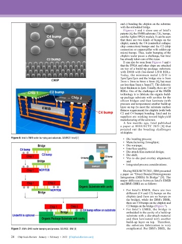
                                                                                Figures 5 and 6 show one of Intel’s
                                                                              patents [6], the EMIB substrate [7,8], bumps,
                                                                              and the Agilex FPGA module. It can be seen
                                                                              that there are two kinds of bumps on the
                                                                              chiplet, namely the C4 (controlled collapse
                                                                              chip connection) bumps and the C2 (chip
                                                                              connection or copper-pillar with solder-cap
                                                                              micro) bumps. Thus, wafer bumping of the
                                                                              chiplets wafer poses a challenge, but Intel
                                                                              has already taken care of this issue.
                                                                                It can also be seen from Figures 5 and 6
                                                                              that the FPGA and other chips are attached
                                                                              on top of a build-up package substrate
                                                                              with EMIB with fine-metal L/S/H RDLs.
                                                                              Today, the minimum metal L/S/H is
                                                                              2μm/2μm/2μm and the bridge size is from
                                                                              2mm x 2mm to 8mm x 8mm [6], but most
                                                                              are less than 5mm x 5mm [7]. The dielectric
                                                                              layer thickness is 2μm. Usually, there are ≤4
                                                                              RDLs. One of the challenges of the EMIB
                                                                              technology is to fabricate the organic build-
                                                                              up package substrate with cavities for the
                                                                              silicon bridges and then laminate (with
                                                                              pressure and temperature) another build-up
                                                                              layer on top (to meet the substrate surface
                                                                              flatness requirement) for chiplets (with both
                                                                              C2 and C4 bumps) bonding. Intel and its
                                                                              suppliers are working toward high-yield
                                                                              manufacturing of the substrate.
                                                                                A few months ago, Intel published
                                                                              a paper at IEEE/ECTC 2021 [8] that
                                                                              pointed out the bonding challenges
                                                                              of chiplets:

        Figure 6: Intel’s EMIB wafer bumping and substrate. SOURCE: Intel [7]   •  Die bonding process;
                                                                                •  Manufacturing throughput;
                                                                                •  Die warpage;
                                                                                •  Interface quality;
                                                                                •  Die attach film material design;
                                                                                •  Die shift;
                                                                                •  Via-to-die-pad overlay alignment;
                                                                                  and
                                                                                •  Integrated process considerations.

                                                                                During IEEE/ECTC2021, IBM presented
                                                                              a paper on “Direct Bonded Heterogeneous
                                                                              Integration (DBHi) Si Bridge” [9]. The
                                                                              major differences between Intel’s EMIB
                                                                              and IBM’s DBHi are as follows:
                                                                                •  For Intel’s EMIB, there are two
                                                                                  different (C4 and C2) bumps on the
                                                                                  chiplets (and there are no bumps on
                                                                                  the bridge), while for IBM’s DBHi,
                                                                                  there are C4 bumps on the chiplets and
                                                                                  C2 bumps on the bridge (Figure 7).
                                                                                •  For  Intel’s  EMIB,  the  bridge  is
                                                                                  embedded in the cavity of a build-up
                                                                                  substrate with a die-attach material
                                                                                  and then laminated with another
                                                                                  build-up layer on top.  Therefore,
                                                                                  the substrate fabrication is very
        Figure 7: IBM’s DHBi wafer bumping and process. SOURCE: IBM [9]           complicated. For IBM’s DBHi, the

        24   Chip Scale Review   January  •  February  •  2022   [ChipScaleReview.com]
        24
   21   22   23   24   25   26   27   28   29   30   31