Page 46 - Chip Scale Review_November December_2021-digital
P. 46
The system’s 2.2x magnification
                                                                              projection lens enables up to a 250mm
                                                                              x 250mm exposure field size, with
                                                                              3µm line/space resolution, ±400ppm
                                                                              mag nif ication compensation and
                                                                              ±100ppm anamorphic magnification
                                                                              compensation, with overlay accuracy
                                                                              better than 1µm.
                                                                                Low lens distortion and accurate
                                                                              step and settle movement are also key
                                                                              to meeting the overlay and uniformity
                                                                              requi rements. Distor t ion i n this
                                                                              system  is  less  than  1μm  across  the
                                                                              250mm exposure field. The system’s
                                                                              stage is driven by 8 motors to ensure
                                                                              accurate step and settle behavior, even
                                                                              when loaded with the weight of the
                                                                              large panel.
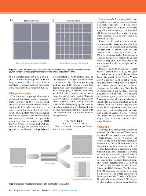
        Figure 3: a) (left) The exposure layout for a 515mm x 510mm panel using a large exposure field (250mm x   During the FOPLP substrate build
        250mm) compared with b) (right) the exposure layout of a smaller field (59mm x 59mm).  process, many layers of RDL and ABF
                                                                              are added to the panel. These films
        and a smaller field (59mm x 59mm)   and Equation 2. With feature sizes in   distort the panel in the X axis, Y axis
        on a 510mm x 515mm panel. With the   the micrometer range, the resolution   and Z axis during thermal cycling.
        large exposure field, the panel can be   requirements for advanced packaging   Magnification compensation allows
        completely exposed with just four shots,   and advanced IC substrates are less   the system to accommodate these
        while the smaller field requires 64 shots.   demanding than requirements for front-  changes in the substrate. Two kinds
                                           end lithography, where feature sizes   of compensation are needed. Isotropic
        Lithography system                 are 1,000 times smaller. At the same   magnification shrinks or enlarges
          The increased topological variation   time, the use of thicker resist films and   the pattern equally in all directions.
        expected for larger panels, physical   larger variations in substrate topography   Anamorphic magnification enlarges or
        distortion  during  the  RDL  build-up   require greater DOF. The projection   shrinks the patterns anisotropically to
        process and the greater feature heights   optics of the lithography system used in   correct for distorted panel registration
        typical of RDL all contribute to the   this demonstration were designed with   errors. Both adjustments are necessary
        requirement for more depth of focus   a lower numerical aperture to meet both   to achieve good overlay and maintain
        (DOF) in the pattern projecting optics. In   the resolution and DOF requirements of   high package yields. Figure 4 shows
        any optical system, DOF and resolution   the application.             the difference bet ween isot ropic
        are inversely related, i.e., gains in                                 m a g n i f i c a t i o n a n d  a n a m o r ph i c
        resolution require sacrifices in DOF       R = k1λ / N.A.  Eq. 1      magnification.
        and vice versa. Resolution and DOF are      DOF = k2λ / N.A.²   Eq. 2
        related through the system’s numerical   Where k1 and k2 are process factors,   Resolution
        aperture, as shown in  Equation 1   and λ is wavelength.                The large-field lithography system was
                                                                              evaluated for CD control of lines/spaces
                                                                              and vias, CD uniformity, and overlay.
                                                                                3µm lines.  Figure 5 shows the
                                                                              results of the 3µm line/space resolution
                                                                              evaluation. A CCL/ABF substrate with a
                                                                              10µm-thick dry film resist was selected
                                                                              for this demonstration, resulting in lines
                                                                              with just over a 1:3 aspect ratio. Best dose
                                                                              and best focus were determined using a
                                                                              focus exposure matrix (FEM). Best dose
                                                                              was used for the resolution demonstration.
                                                                              The figure indicates that CDs showed
                                                                              less than 10% deviation from -10μm to
                                                                              -70μm, at a DOF of 60μm. The data from
                                                                              the FEM were used to generate a Bossung
                                                                              plot (Figure 5a) in which the X-axis is
                                                                              focus (μm) and the Y-axis is CD (μm).
                                                                              The plot shows the 60μm DOF. Figure
                                                                              5b also includes a lower magnification
        Figure 4: Isotropic magnification and anamorphic magnification compensation.

        44
        44   Chip Scale Review   November  •  December  •  2021   [ChipScaleReview.com]

