Page 48 - Chip Scale Review_November December_2021-digital
P. 48

of the second layer included site-by-site
                                                                              correction for each exposure field. Overlay
                                                                              error was checked by reading overlapped
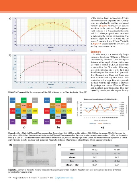
                                                                              verniers (Figure 9) included at certain
                                                                              locations in the patterns. Each exposure
                                                                              field contains 3 x 3 measurement points;
                                                                              and 2 x 2 shots per panel were measured
                                                                              to determine the overlay performance. The
                                                                              mean +3 sigma in X was 0.91µm, and the
                                                                              mean +3 sigma in Y was 0.91µm. The table
                                                                              in Figure 9 summarizes the results of the
                                                                              overlay error measurements.

                                                                              Summary
                                                                                In this study, an extremely large
                                                                              exposure field size (250mm x 250mm)
                                                                              successfully resolved 3µm line/space
                                                                              features with a depth of focus >60µm on
                                                                              a 510mm x 515mm CCL/ABF stack with
                                                                              a 10µm-thick dry film resist. This study
                                                                              also demonstrated successful 5µm and
                                                                              6µm line/space features with a 25µm-thick
                                                                              dry film resist and 15µm and 20µm vias
                                                                              with a 40µm-thick dry film resist. Fine
                                                                              resolution and a large field size provide
                                                                              the user with the opportunity to increase
                                                                              the package size beyond 150mm x 150mm
                                                                              and maintain high throughput. This new
                                                                              capability has the potential to pave the way
        Figure 7: a) Bossung plot for 15μm vias showing 110μm DOF. b) Bossung plot for 20μm vias showing 110μm DOF.


        Figure 8: a) 3µm CD plot in 250mm x 250mm exposure field: The maximum CD is 3.258µm, and the minimum CD is 2.988µm; the average CD is 3.099µm, and the
        uniformity is 4.32%. b) 3µm CD deviation contribution map in 250mm x 250mm exposure field: The center location has a minimum deviation of -0.20% and the deviation
        trend up to 2.2% to 4.12% at corner locations, the maximum deviation is 4.12%, which is at the top-right corner. Overall, the deviation meets our expectation. c) 3µm CD
        and CD deviation chart: No trending or peak is observed. This chart indicates the CD performance with a 250mm x 250mm exposure field is stable.


        Figure 9: A summary of the results of overlay measurements: a) Overlapped verniers included in the pattern were used to measure overlay errors. b) The table
        summarizes the measured errors.

        46
        46   Chip Scale Review   November  •  December  •  2021   [ChipScaleReview.com]
   43   44   45   46   47   48   49   50   51   52   53