Page 47 - Chip Scale Review_November December_2021-digital
P. 47
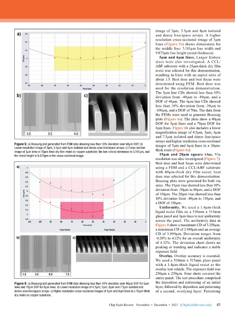
image of 3μm, 3.5μm and 4μm isolated
                                                                              and dense line/space arrays. A higher
                                                                              resolution cross-sectional image of 3μm
                                                                              lines (Figure 5c) shows dimensions for
                                                                              the middle line: 3.181µm line width and
                                                                              9.873µm line height (resist thickness).
                                                                                5µm and 6µm lines. Larger feature
                                                                              sizes were also investigated. A CCL/
                                                                              ABF substrate with a 25µm-thick dry film
                                                                              resist was selected for this demonstration,
                                                                              resulting in lines with an aspect ratio of
                                                                              about 1:5. Best dose and best focus were
                                                                              determined using FEM. Best dose was
                                                                              used for the resolution demonstration.
                                                                              The 5μm line CDs showed less than 10%
                                                                              deviation from -40μm to -80μm, and a
                                                                              DOF of 40μm. The 6μm line CDs showed
                                                                              less than 10% deviation from -30μm to
                                                                              -100μm, and a DOF of 70m. The data from
                                                                              the FEMs were used to generate Bossung
                                                                              plots (Figure 6a). The plots show a 40μm
                                                                              DOF for 5μm lines and a 70μm DOF for
                                                                              6μm lines. Figure 6b also includes a lower
                                                                              magnification image of 4.5μm, 5μm, 6μm
                                                                              and 7.5μm isolated and dense line/space
                                                                              arrays and higher resolution cross-sectional
        Figure 5: a) Bossung plot generated from FEM data showing less than 10% deviation over 60μm DOF; b)   images of 5μm and 6μm lines in a 10μm-
        Lower resolution image of 3μm, 3.5μm and 4μm isolated and dense area line/space arrays; c) Cross-section   thick resist (Figure 6c).
        image of 3µm lines in 10µm thick dry film resist on copper substrate; the line critical dimension is 3.181µm, and
        the resist height is 9.873µm in the cross-sectional image.              15µm and 20µm square vias. Via
                                                                              resolution was also investigated (Figure 7).
                                                                              Best dose and best focus were determined
                                                                              using a FEM and a CCL/ABF substrate
                                                                              with 40µm-thick dry film resist; best
                                                                              dose was selected for this demonstration.
                                                                              Bossung plots were generated for both via
                                                                              sizes. The 15μm vias showed less than 10%
                                                                              deviation from -30μm to 80μm, and a DOF
                                                                              of 110μm. The 20μm vias showed less than
                                                                              10% deviation from -40μm to 110μm, and
                                                                              a DOF of 150μm.
                                                                                Uniformity. We used a 1.4µm-thick
                                                                              liquid resist film on a 510mm x 515mm
                                                                              glass panel and 3µm lines to test uniformity
                                                                              across the panel. The uniformity data in
                                                                              Figure 8 show a maximum CD of 3.258μm,
                                                                              a minimum CD of 2.988μm and an average
                                                                              CD of 3.099μm. Deviation ranges from
                                                                              -0.20% to 4.12% for an overall uniformity
                                                                              of 4.32%. The deviation chart shows no
                                                                              peaking or trending and indicates a stable
                                                                              exposure field.
                                                                                Overlay. Overlay accuracy is essential.
                                                                              We used a 510mm x 515mm glass panel
                                                                              with a 1.4µm-thick liquid resist as the
                                                                              overlay test vehicle. The exposure field was
                                                                              250µm x 250µm. Four shots covered the
                                                                              entire panel. The test procedure comprised
        Figure 6: a) Bossung plot generated from FEM data showing less than 10% deviation over 40μm DOF for 5μm   the deposition and patterning of an initial
        lines and 70μm DOF for 6μm lines. b) Lower resolution image of 4.5μm, 5μm, 6μm and 7.5μm isolated and   layer, followed by deposition and patterning
        dense area line/space arrays. c) Higher resolution cross-sectional images of 5μm and 6μm lines in a 10μm-thick   of a second, overlying layer. Patterning
        dry resist on copper substrate.

                                                                                                             45
                                                       Chip Scale Review   November  •  December  •  2021   [ChipScaleReview.com]  45

