Chip Scale Review January February 2020 Volume 24, Number 1
Wafer geometry is vital for process control at the front end of line, and ultimately, device yield. Additionally, as wafer thinning becomes ever more critical at the far back end of line, so too, is being able to quickly measure wafer geometry (e.g., nanotopography, roughness) on the entire wafer. Not only has wavefront phase imaging been shown to be a good candidate for FEOL and FBEOL applications, it is also showing promise for global wafer geometry measurements on patterned wafers during BEOL processes.
Photo courtesy of iStock/Norman Cooper
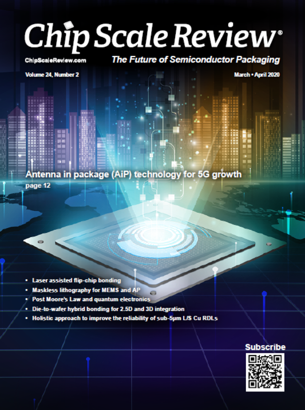
Chip Scale Review March April 2020 Volume 24, Number 2
Implementing 5G technology requires transmission of large amounts of data, reliable connections, quicker response time, and better coverage. Fully integrated RF front-end modules using a system in package (SiP) that includes antenna in package (AiP) technology, double-sided assembly, advanced wafer-level redistribution layer (RDL), passive component integration, and sophisticated RF shielding techniques provide the most advanced 5G package.
Chip Scale Review May June 2020 Volume 24, Number 3
The requirements for back-end lithography continue to grow as heterogeneous integration becomes an increasing driving force in semiconductor development and innovation. The increased importance of design flexibility, minimizing pattern
distortion and die shifts in advanced packaging, reducing consumable costs, supporting both thick and thin resists, and shortening development cycles between R&D and production, are just a few factors driving the need for maskless exposure (MLE) technology.
Chip Scale Review July August 2020 Volume 24, Number 4
The 5G rollout is underway, exponentially spurred on by COVID-19 and the new data requirements for video conferencing, meetings, and virtual conferences, as millions of people around the world work from home. The reality of both increased demand for faster connections and higher bandwidth to handle the larger volumes of data passing through networks must be met with attractive solutions. RF GaN power amplifiers enable faster speeds, lower latency, and missioncritical applications. A low-void die attach process of 1% or less for GaN dies plays a crucial role in achieving these benefits.
Chip Scale Review September October 2020 Volume 24, Number 5
The market growth in advanced driver assistance systems, electric vehicles and autonomous vehicle technologies is driving the need for a zero defects strategy in the manufacture of ICs. Implementing such a strategy will require a holistic approach to automation that also meets the investment constraints facing legacy manufacturing facilities.
Chip Scale Review November December 2020 Volume 24, Number 6
AI makes very large demands on compute, memory and bandwidth requirements. As such, AI has provided a major incentive for deployment of specialized components whereby heterogeneous integration has risen to the forefront as a way to enable high interconnectivity among them. Additionally, heterogeneous integration helps counter the diminishing returns of scaling.
In 2020, Chip Scale Review had its ongoing focus on the technologies that facilitated the evolution of semiconductor performance in all of the categories that were of meaningful significance. Industry experts heeded Chip Scale Review’s call for QC/AI/next-generation computing content, and as a result, we were able to publish several relevant articles in 2020 that included: 1) “Post-Moore’s Law electronics: now, until quantum electronics,” (R. Tummala/Georgia Tech, Mar/Apr) 2) AI’s impact on 3D packaging: heterogeneous integration,” (S. Kumar/ Yole Développement, Korea, May/June); 3) “Electronic packaging for future electronic systems,” (M. Töpper, T. Braun, R. Aschenbrenner/Fraunhofer IZM, Jul/Aug); 4) “Enabling AI with heterogeneous integration,” (N. Fan/ ASM Pacific Technology Ltd., Sept/Oct); 5) “A deep-learning solution for heterogeneous package inspection,” (S. Chitchian/INTEKPLUS Corporation Ltd., Sept/Oct); and 6) “Enabling AI with heterogeneous integration,” (A. Kumar, M. Farooq/IBM Research, Nov/Dec).