Page 8 - ChipScale_Nov-Dec_2020-digital
P. 8
package. With its mature InFO product
                                                                              line-up, and increased investment in
                                                                              SoIC package infrastructure along with
                                                                              the chiplet paradigm shift over the next
                                                                              3-5 years, TSMC is in a good position
                                                                              to take advantage of the heterogeneous
                                                                              integration revolution.
                                                                                UMC is a key supplier of Si interposer
                                                                              for 2.5D packaging. It recently partnered
                                                                              with Xperi to optimize and commercialize
                                                                              ZiBond and DBI technologies for a
                                                                              wide range of semiconductor devices,
                                                                              including image sensors, radio frequency
                                                                              (RF), microelectromechanical systems
                                                                              ( M EMS), d isplay d r iver s, touch
                                                                              controllers, SoC, analog, power and
                                                                              mixed-signal devices. ZiBond and DBI
                                                                              support wafer-to-wafer (W2W) and
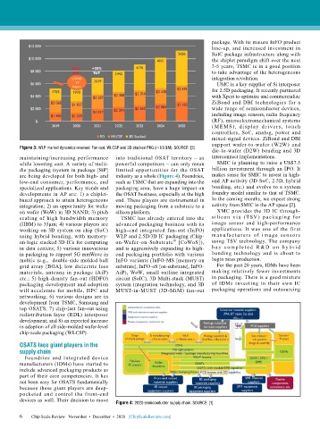
        Figure 3: WLP market dynamics revenue: Fan-out, WLCSP and 3D stacked PKG (in US $M). SOURCE: [3]
                                                                              die-to-wafer (D2W) bonding and 3D
        maintaining/increasing performance   into traditional OSAT territory – as   interconnect implementations.
        while lowering cost. A variety of multi-  powerful competitors – can only mean   SMIC is planning to raise a US$7.5
        die packaging (system in package [SiP]   limited opportunities for the OSAT   billion investment through an IPO. It
        are being developed for both high- and   industry as a whole (Figure 4). Foundries,   makes sense for SMIC to invest in high-
        low-end consumer, performance, and   such as TSMC that are expanding into the   end AP activity (3D SoC, 2.5D, hybrid
        specialized applications. Key trends and   packaging area, have a huge impact on   bonding, etc.) and evolve to a system
        developments in AP are: 1) a chiplet-  the OSAT business, especially at the high   foundry model similar to that of TSMC.
        based approach to attain heterogeneous   end. These players are instrumental in   In the coming months, we expect strong
        integration; 2) an opportunity for wafer   moving packaging from a substrate to a   activity from SMIC in the AP space [2].
        on wafer (WoW) in 3D NAND; 3) pitch   silicon platform.                 XMC provides the 3D IC through-
        scaling of high bandwidth memory     TSMC has already entered into the   silicon via (TSV ) packagi ng for
        (HBM) to 35µm; 4) various players are   advanced packaging business with its   image sensor and high-performance
        working on 3D system on chip (SoC)   high-end integrated fan-out (InFO)   applications. It was one of the first
        using hybrid bonding, with memory-  WLP and 2.5D/3D IC packaging (Chip-  ma nufact u rers of i mage sensors
                                                                 ®
        on-logic stacked 3D-ICs for computing   on-Wafer-on-Substrate  [CoWoS]),   using TSV technology. The company
        in data centers; 5) various innovations   and is aggressively expanding its high-  h a s c o m p l e t e d R &D o n h y b r i d
        in packaging to support 5G mmWave in   end packaging portfolio with various   bonding technology and  is about  to
        mobile (e.g.,  double-side molded ball   InFO variants (InFO-MS [memory on   begin mass production.
        grid array [BGA], low dielectric loss   substrate], InFO-oS [on-substrate], InFO-  For the past 20 years, IDMs have been
        materials, antenna in package (AiP)   AiP), WoW, small outline integrated   making relatively fewer investments
        etc.; 5) high-density fan-out (HDFO)   circuit (SoIC), 3D Multi-stack (MUST)   in packaging. There is a good mixture
        packaging development and adoption   system integration technology, and 3D   of IDMs investing in their own IC
        will accelerate for mobile, HPC and   MUST-in-MUST (3D-MiM) fan-out   packaging operations and outsourcing
        networking; 6) various designs are in
        development from TSMC, Samsung and
        top OSATS; 7) chip-last fan-out using
        redistribution layer (RDL) interposer
        development; and 8) an expected increase
        in adoption of all side-molded wafer-level
        chip-scale packaging (WLCSP).

        OSATS face giant players in the
        supply chain
          Foundries and integrated device
        manufacturers (IDMs) have started to
        include advanced packaging products as
        part of their core competencies. It has
        not been easy for OSATS fundamentally
        because these giant players are deep-
        pocketed and control the front-end
        devices as well. Their decision to move
                                           Figure 4: 2020 semiconductor supply chain. SOURCE: [1]

        6 6  Chip Scale Review   November  •  December  •  2020   [ChipScaleReview.com]

