Page 7 - ChipScale_Nov-Dec_2020-digital
P. 7
The future of OSATS


        By Favier Shoo, Santosh Kumar  [Yole Développement]
        O          ver the past few decades,


                   the integrated circuit (IC)
                   industry has been relying on
                   traditional chip scaling and
        innovative architectures for new devices,
        closely following Moore’s Law. In die-
        level scaling, the idea is to pack ever more
        transistors on a monolithic die or system
        on a chip (SoC) with the development of
        each front-end process node, enabling faster
        chips with a lower cost per transistor. With
        traditional die-level scaling, however, the
        design cost has risen many times (e.g., 3nm
        design costs ~35-40X more compared to
        90nm) and manufacturing has become
        extremely complex, leading to an increase
        in time to market. Therefore, it is widely   Figure 1: Semiconductor packaging value roadmap. SOURCE: [1]
        acknowledged that Moore’s Law is slowing
        down, if not dead.
          While front-end scaling remains a work
        in progress in the background, the industry
        has been diligently leveraging on packaging
        technologies to improve system-level
        interconnection density and reduce the cost
        and time to market by scaling the package-
        level pitch and integrating more functions
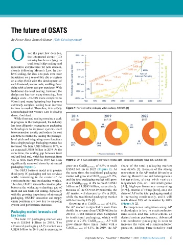
        into a single package. Packaging revenue has
        increased 70x from US$1 billion in 1970, to
        an expected US$68 billion in 2019. At the
        same time, the scaling gap between front
        end and back end, which has increased from
        50x to 600x from 1970 to 2019, has been   Figure 2: 2014-2025 packaging overview in revenue split - advanced packaging focus ($B). SOURCE: [1]
        significantly narrowed down by advanced
        packaging (Figure 1).              grow at a CAGR 2019-2025  of 6.6% to reach   share of the total packaging market
          The OSAT business model is to provide   US$42 billion in 2025 (Figure 2). At   was 42.6% [1]. Because of the strong
        third-party IC packaging and test services   the same time, the traditional packaging   momentum in the AP market driven by a
        while remaining in the center of the   market will grow at a CAGR 2019-2025  of 1.9%,   slowing Moore’s Law and heterogeneous
        semiconductor and packaging worlds.   and the total packaging market will grow   i nt eg r at ion , a long w it h va r iou s
        Therefore, OSATS remain the essential pillar   at a CAGR 2019-2025  of 4% to reach US$43   megatrends (5G, artificial intelligence
        between the widening technology gap of   billion and US$85 billion, respectively.   [AI], high-performance computing
        front-end and back-end scaling. Especially   Because of the COVID-19 pandemic, the   [HPC], Internet of Things [IoTs], etc.), the
        with the growing importance of advanced   AP market will decrease by 7% in 2020,   share of AP in the total packaging market
        packaging, OSATS’ innovation and supply   while the traditional packaging market   is increasing continuously, and it will
        chain positions are now key to on-going   will decrease by 15% [1].   reach almost 50% of the market by 2025
        system-level performance increases.  Growing at a CAGR 2014-2025  of 6.1%,   (Figure 3) [2].
                                           the AP market is expected to more than   Heterogeneous integration using AP
        Packaging market forecasts and     double its revenue from US$20 billion in   technologies is key to semiconductor
        key trends                         2014 to ~US$4 billion in 2025. Compared   innovation and the achievement of
          The total IC packaging market was   to traditional packaging, which will   desired system performance. Advanced
        worth US$68 billion in 2019. The   grow at a 2.2% CAGR 2014-2025 , AP will   semiconductor packaging is seen to
        advanced packaging (AP) market was   grow almost three times  faster with a   increase the value of a semiconductor
        US$38 billion in 2019 and is expected to   CAGR 2014-2025  of 6.1%. In 2019, the AP   product,  adding  functionality  and

                                                       Chip Scale Review   November  •  December  •  2020   [ChipScaleReview.com]  5 5

