Page 41 - Chip Scale Review_November-December_2023-digital
P. 41
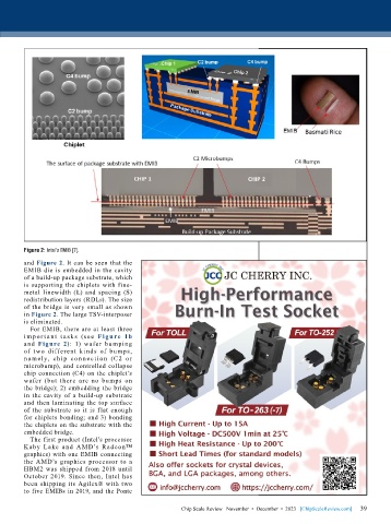
Figure 2: Intel’s EMIB [7].
        and Figure 2. It can be seen that the
        EMIB die is embedded in the cavity
        of a build-up package substrate, which
        is supporting the chiplets with fine-
        metal linewidth (L) and spacing (S)
        redistribution layers (RDLs). The size
        of the bridge is very small as shown
        in Figure 2. The large TSV-interposer
        is eliminated.
          For EMIB, there are at least three
        i mp or t a nt t a sk s (se e  F i g u re 1b
        and  Figure 2): 1) wafer bumping
        of two different kinds of bumps,
        na mely, ch ip con ne ct ion (C2 or
        microbump), and controlled collapse
        chip connection (C4) on the chiplet’s
        wafer (but there are no bumps on
        the bridge); 2) embedding the bridge
        in the cavity of a build-up substrate
        and then laminating the top surface
        of the substrate so it is flat enough
        for chiplets bonding; and 3) bonding
        the chiplets on the substrate with the
        embedded bridge.
          The first product (Intel’s processor
        Kaby Lake and AMD’s Radeon™
        graphics) with one EMIB connecting
        the AMD’s graphics processor to a
        HBM2 was shipped from 2018 until
        October 2019. Since then, Intel has
        been shipping its Agilex® with two
        to five EMIBs in 2019, and the Ponte

                                                                                                             39
                                                       Chip Scale Review   November  •  December  •  2023   [ChipScaleReview.com]  39

