Page 40 - Chip Scale Review_November-December_2023-digital
P. 40
Recent advances in bridges for chiplets communications


        By John H. Lau  [Unimicron Technology Corporation]
        R         e c e n t l y , b e c a u s e  o f   printed circuit board (PCB) with ball   TSV-interposer (>160mm x 160mm


                                                                                          2
                  t he d r ive of a r t i f icia l
                                                                              Conference on August 29, 2023.
                  i ntell igence (A I ) such   grid array (BGA) solder balls and   = 25,600mm ) at the IEEE Hot Chip
                                           solder  paste. This  multiple  chiplet
        as Open AI’s GPT, generative AI    system and heterogeneous integration   TSMC  called  2.5D  IC  integration
        and conversational AI, and 5G/6G,   packaging are driven by performance   c h i p - on - w a f e r - on - s u b s t r a t e
                                                                                      ®
        t h e a p p l i c a t i o n s s u c h a s h i g h -  and form factor and for extremely   (CoWoS ).  T he  2.5D  or  3D  w it h
        p e r for m a nc e c omput i ng ( H PC),   high-density and high-performance   TSV-i nter poser  is  k now n  for  its
        autonomou s veh icle, i nter net of   applications [4].               high cost. One of the key reasons
        things (IoTs), big data (for cloud   The very first 2.5D IC integration   for its high cost is because the TSV-
        computing) and instant data (for edge   papers were published by CEA-Leti   interposer manufacturing (with the
        computing) are demanding more      [5] at IEEE/ECTC 2005 and [6] at   64nm process technology) yield loss
        advanced semiconductor packaging    IEEE/ECTC 2006. The ver y f irst   is  high  because  of  its  large  size.
        technology [1-3].                  product (Virtex™-7 HT family) of   The objective of this brief note is to
          One of the most popular advanced   2.5D was shipped in 2013 by Xilinx   present some of the recent advances
        packaging technologies is the 2.5D or   and TSMC. Since then, AMD shipped   in using silicon bridges to replace the
        3D integrated circuit (IC) integration   its Radeon™ R9 Fury X GPU, Nvidia   TSV-interposer.
        [4] as schematically shown in Figure   s h i p p e d i t s P a s c a l ™ 10 0 G PU,
        1a. It can be seen that the system   Fujitsu shipped its Fugaku (A64FX   Intel’s embedded multi-die
        on chip (SoC) devices, such as the   CPU), and Graphcore shipped Bow   interconnect bridge (EMIB)
        central  processing  unit  (CPU)  and   (an intelligence processing unit),   At IEEE ECTC 2016, Intel published
        graphics processing unit (GPU), and   etc.  Very  recently,  Nvidia  shipped   the first paper on bridge for chiplets
                                                                 2
        h ig h-ba ndw idt h memor y ( H BM )   its A100 GPU (826mm ) with six   communication [7]. One of the key
        are supported by a passive (2.5D)   HBM2 suppor ted by a ver y large   objectives of the paper was to show
        or active (3D) through-silicon via   TSV-inter poser and AMD/Xilinx   the replacement of the TSV-interposer
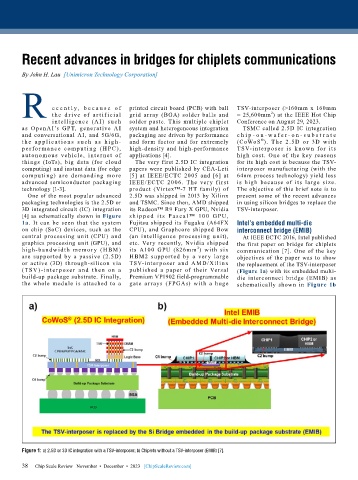
        (TSV ) -i nte r pose r a nd t hen on a   published a paper of their Versal   (Figure 1a) with its embedded multi-
        build-up package substrate. Finally,   Premium VP1902 field-programmable   die interconnect bridge (EMIB) as
        the whole module is attached to a   gate ar rays (FPGAs) with a huge   schematically  shown  in  Figure  1b


        Figure 1: a) 2.5D or 3D IC integration with a TSV-interposer; b) Chiplets without a TSV-interposer (EMIB) [7].

        38
        38   Chip Scale Review   November  •  December  •  2023   [ChipScaleReview.com]

