
Page 26 - Chip Scale Review_July August_2023-digital
P. 26
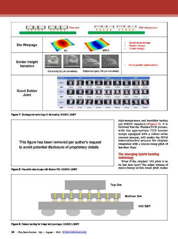
Figure 7: Challenges for extra-large HI die bonding. SOURCE: ASMPT
                                                                              high-temperature and humidity testing
                                                                              per JEDEC standard (Figure 9). It is
                                                                              believed that the fluxless-TCB process,
                                                                              with the appropriate TCB bonder
                                                                              design equipped with a robust oxide
                                                                              removal process, will enable the HVM
                                                                              interconnection process for chiplets
             This figure has been removed per author's request
                                                                              integration with a micron bump pitch of
             to avoid potential disclosure of proprietary details             less than 10µm.
                                                                              The emerging hybrid bonding
                                                                              technology
                                                                                What if the chiplets’ I/O pitch is to
                                                                              be less than 1µm? The solder volume of
                                                                              micro-bumps at this small pitch makes
        Figure 8: Fine-pitch micro bumps with fluxless-TCB. SOURCE: ASMPT


        Figure 9: Fluxless bonding for 2-layer stack packages. SOURCE: ASMPT

        24
        24   Chip Scale Review   July  •  August  •  2023   [ChipScaleReview.com]