Page 25 - Chip Scale Review_July August_2023-digital
P. 25

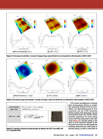
Figure 4: HI die warpage characterization. An example of warpage in large compound HI dies from room temperature to reflow temperature. SOURCE: ASMPT


        Figure 5: HDI substrate warpage characterization. An example of warpage in a large HDI substrate from room temperature to reflow temperature. SOURCE: ASMPT
                                                                                TCB bonder manufacturers continue
                                                                              their development efforts to enable
                                                                              the emerging fluxless-TCB process,
                                                                              which is an alternative process to very
                                                                              expensive and yet HVM immature
                                                                              hybrid bonding (HB) technology. Recent
                                                                              development work has shown robust
                                                                              bonding capability for micro bump
                                                                              devices with fine bump pitch at less than
                                                                              15µm (Figure 8). The test vehicle, in the
                                                                              form of a 3D structure bonded by the
                                                                              fluxless-TCB process, has also passed the
                                                                              reliability stress test up to 1000 cycles of
        Figure 6: HI packaging architecture associated challenges and solutions with ASMPT home-built TV with    thermal cycling, as well as 1000 hours of
        70 x 70 integrated die size.

                                                                                                             23
                                                             Chip Scale Review   July  •  August  •  2023   [ChipScaleReview.com]  23
   20   21   22   23   24   25   26   27   28   29   30