
Page 22 - Chip Scale Review_July August_2023-digital
P. 22
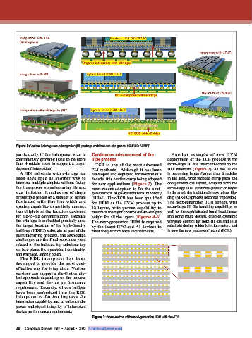
Figure 2: Various heterogeneous integration (HI) package architectures at a glance. SOURCE: ASMPT
        particularly if the interposer size is   Continuous advancement of the   A nother example of new H V M
        continuously growing (said to be more   TCB process                   deployment of the TCB process is for
        than 4 reticle sizes to support a larger   TCB is one of the most advanced   extra-large HI die interconnection to the
        degree of integration).            FLI methods.  Although it has been   HDI substrate (Figure 7). As the HI die
          A HDI substrate with e-bridge has   developed and deployed for more than a   is becoming larger (larger than 6 reticles
        been developed as another way to   decade, it is continuously being adopted   in the area), with reduced bump pitch and
        integrate multiple chiplets without facing   for new applications (Figure 3). The   complicated die layout, coupled with the
        the interposer manufacturing format   most recent adoption is for the next-  extra-large HDI substrate (easily 2x larger
        size limitation. It makes use of single   generation high-bandwidth memory   in the area), the traditional mass reflow flip-
        or multiple pieces of a smaller Si bridge   (HBM). Flux-TCB has been qualified   chip (MR-FC) process becomes impossible.
        fabricated with fine line width and   for HBM as the HVM process up to   The next-generation TCB bonder, with
        spacing capability to partially connect   12 layers, with proven capability to   extra-large HI die handling capability, as
        two chiplets at the location designed   maintain the tight control die-to-die gap   well as the sophisticated bond head heater
        for die-to-die communication. Because   height for all the layers (Figures 4-6).   and bond stage design, enables dynamic
        the e-bridge is embedded precisely onto   The next-generation HBM is required   warpage control for both HI die and HDI
        the target location of the high-density   by the latest HPC and AI devices to   substrate during solder joint formation, and
        build-up (HDBU) substrate as part of the   meet the performance requirements.  is now the new process of record (POR).
        manufacturing process, the associated
        challenges are the final substrate yield
        related to the induced top substrate top
        surface planarity, open/short continuity,
        and warpage, among others.
          T he R DL i nt e r p ose r h a s b e e n
        developed to provide the most cost-
        effective way for integration. Various
        versions can support a die-first or die-
        last approach depending on the process
        capability  and  device  performance
        requirement. Recently, silicon bridges
        have been embedded into the RDL
        interposer to further improve the
        integration capability and to enhance the
        power and signal integrity of integrated
        device performance requirements.
                                           Figure 3: Cross-section of the next-generation HBM with flux-TCB.

        20   Chip Scale Review   July  •  August  •  2023   [ChipScaleReview.com]
        20