
Page 18 - Chip Scale Review_July August_2023-digital
P. 18
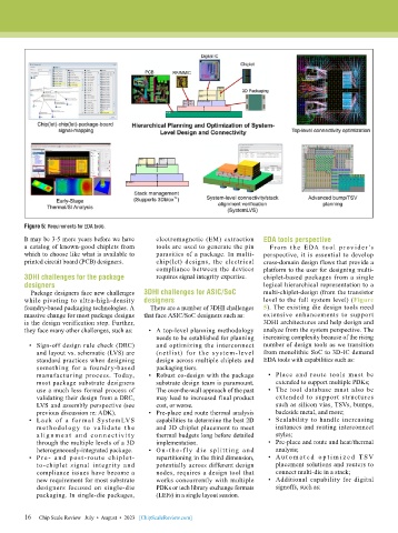
Figure 5: Requirements for EDA tools.
        It may be 3-5 more years before we have   electromagnetic (EM) extraction   EDA tools perspective
        a catalog of known-good chiplets from   tools are used to generate the pin   From t he EDA tool prov ide r’s
        which to choose like what is available to   parasitics of a package. In multi-  perspective, it is essential to develop
        printed circuit board (PCB) designers.  chip(let) designs, the electrical   cross-domain design flows that provide a
                                               compliance between the devices   platform to the user for designing multi-
        3DHI challenges for the package        requires signal integrity expertise.  chiplet-based packages from a single
        designers                                                             logical hierarchical representation to a
          Package designers face new challenges   3DHI challenges for ASIC/SoC   multi-chiplet-design (from the transistor
        while pivoting to ultra-high-density   designers                      level to the full system level) (Figure
        foundry-based packaging technologies. A   There are a number of 3DHI challenges   5). The existing die design tools need
        massive change for most package designs   that face ASIC/SoC designers such as:  extensive enhancements to support
        is the design verification step. Further,                             3DHI architectures and help design and
        they face many other challenges, such as:  •  A top-level planning methodology   analyze from the system perspective. The
                                               needs to be established for planning   increasing complexity because of the rising
          •  Sign-off design rule check (DRC)   and optimizing the interconnect   number of design tools as we transition
            and layout vs. schematic (LVS) are   (netlist) for the system-level   from monolithic SoC to 3D-IC demand
            standard practices when designing   design across multiple chiplets and   EDA tools with capabilities such as:
            something for a foundry-based      packaging tiers.
            manufacturing process. Today,    •  Robust co-design with the package   •  Place and route tools must be
            most package substrate designers   substrate design team is paramount.   extended to support multiple PDKs;
            use a much less formal process of   The over-the-wall approach of the past   •  The tool database must also be
            validating their design from a DRC,   may lead to increased final product   extended to support structures
            LVS and assembly perspective (see   cost, or worse.                   such as silicon vias, TSVs, bumps,
            previous discussion re: ADK).    •  Pre-place and route thermal analysis   backside metal, and more;
          •  Lack of a for mal System LVS      capabilities to determine the best 2D   •  Scalability to handle increasing
            met hodolog y to val id at e t he   and 3D chiplet placement to meet   instances and routing interconnect
            a l ig n m e nt  a n d  c o n n e c t iv it y   thermal budgets long before detailed   styles;
            through the multiple levels of a 3D   implementation.               •  Pre-place and route and heat/thermal
            heterogeneously-integrated package.   •  O n-t he -f ly d ie spl it t i ng a nd   analysis;
          •  P re - a nd p ost-rout e ch iplet-  repartitioning in the third dimension,   •  A u to m a t ed  o p t i m i z ed  T S V
            to-chiplet  signal  integrity  and   potentially across different design   placement solutions and routers to
            compliance issues have become a    nodes, requires a design tool that   connect multi-die in a stack;
            new requirement for most substrate   works concurrently with multiple   •  Additional capability for digital
            designers focused on single-die    PDKs or tech library exchange formats   signoffs, such as:
            packaging. In single-die packages,   (LEFs) in a single layout session.


        16   Chip Scale Review   July  •  August  •  2023   [ChipScaleReview.com]
        16