
Page 15 - Chip Scale Review_July August_2023-digital
P. 15
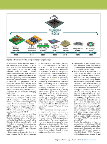
Figure 2: Heterogeneous integration leverages multiple packaging technologies.
        were multi-die packaging using foundry-  of an ASIC/SoC into smaller building   •  Convergence of the die design flows
        based manufacturing techniques. A few   blocks, each of which can be fabricated   with the system design flows leads to
        years later, foundries also started offering   at what eve r node or t e ch nolog y   questions about the expertise needed
        higher-density single-die packaging   makes the most sense. Advanced      (die design or system design).
        solutions ideally suited for the mobile   packaging then becomes the process   •  While using bumpless stacking
        communications market. Fan-out wafer-  of aggregating all the building blocks   technology, in many cases, true
        level packaging (FOWLP) wasn’t new, but   (chiplets). And, of course, designers get   chip-on-wafer and wafer-on-wafer
        the ultra-high-density fan-out redistribution   to choose from dozens of packaging   applications are not packaging at all.
        layer (RDL) provided smaller interconnect   technologies (Figure 2). As discussed   Instead, it’s die design except with the
        geometries than previous FOWLP     previously, semiconductor foundries    ability to now design in the vertical
        solutions. These new foundry-based   started extending the back-end design   direction. This silicon stacking
        technologies created healthy competition   services into silicon-based advanced   approach best suits the die designer
        and collaboration with the outsourced   packaging solutions a decade ago. The   with enhanced 3D capabilities in
        semiconductor assembly and test (OSAT)   foundry-based approach of high-density   their place and route tool. In most
        companies that had dominated packaging   interconnect  geometries  combined   cases, silicon stacking doesn’t use
        for 25 years.                      with TSVs paved the way for silicon    chiplets in the traditional sense.
          Over the past few years, a new   interposers to emerge as the leading   Instead, a single register transfer
        vernacular has emerged based on a new   technology to aggregate and integrate   level (RTL) gets partitioned in the
        set of acronyms – 3DHI, 3D-IC, and   multiple chiplets. But other packaging   third dimension, and in the case of
        chiplets. This new vernacular primarily   technologies might be starting to catch   face-to-face stacking, small 1-2µm
        comes from semiconductor foundries   up. Most notable are RDL interposers,   pads are used to connect the two
        and IC designers as they pivot from More   which don’t require TSVs, thus lowering   levels. This differs from most chiplet-
        Moore to the world of More-Than-Moore   the cost.                         based applications, which connect
        (3DHI). The sections below discuss   With advanced packaging as the       devices with micro I/O buffers, RDL,
        specific challenges with 3DHI.     pr imar y tech nolog y for the next    and micro-bumps using a die-to-
          3D heterogeneous integration     generation  of elect ronic product     die (D2D) communication interface
        (3DHI). Heterogeneous integration is   design, it’s crucial to understand the   such as Unified Chiplet Interconnect
        about the disaggregation of a chip into   nuances between different packaging   Express (UCIe™) or bunch of
        smaller building blocks, commonly called   technologies. Packaging engineers   wires (BoW).
        chiplets. It offers many benefits, such   have been designing organic/laminate   •  Finally, the combination of these two
        as: 1) Lower nonrecurring engineering   substrates for three decades. The design   worlds is the hybrid scheme. Hybrid
        ( N R E) costs; 2) Shor ter t i me to   f lows and methodologies are well   packaging technologies combine these
        market (TTM); and 3) Flexibility and   established. However, some interesting   two worlds (3D packaging and silicon
        modularization benefits.           facts about today’s foundry-based      stacking). 2.5D silicon interposer or
          Heterogeneous integration is a term   packaging technologies include:   ultra-high-density FOWLP requires
        used to describe the disaggregation                                       tools and expertise spanning IC and


                                                                                                             13
                                                             Chip Scale Review   July  •  August  •  2023   [ChipScaleReview.com]  13