
Page 12 - Chip Scale Review_July August_2023-digital
P. 12
Transitioning from 3D packaging to 3D heterogeneous
integration (3DHI)
By John Park, Vinod Kumar Khera [Cadence Design Systems]
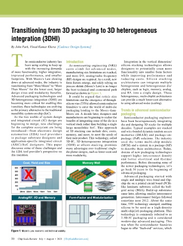
T he semiconductor industry has Introduction Integration in the vertical dimension/
been using scaling to keep up
As nonrecurring engineering (NRE)
with the increasing demands costs climb for advanced nodes, silicon stacking technologies allows
designers to potentially cram more
of more functionality, higher integration, manufacturing size limitations are reached, functionality into smaller form factors
improved performance, and smaller and more I/O, analog/radio frequency while improving performance and
footprints. With Moore’s Law slowing (RF) designs are required. As a result, new reducing costs. Silicon st ack ing
down at advanced nodes, the industry is form factors emerge, and solely relying on architectures can integrate multiple
transitioning from “More Moore” to “More process shrink (Moore’s Law) is no longer homogeneous and heterogeneous die/
Than Moore” for the lower cost, larger the best technical and economical path chiplets, such as logic, memory, analog,
design sizes and modularity benefits. forward as shown in Figure 1. and RF, into a single design. These
Advanced packaging technologies and It could be argued that reticle size heterogeneous, multi-chiplet architectures
3D heterogeneous integration (3DHI) are limitations and the emergence of through- can provide a much lower-cost alternative
becoming more critical for enabling this silicon vias (TSVs) allowed semiconductor to using advanced nodes (scaling).
transition; these technologies are evolving foundries to enter the world of multi-die
as the primary alternative to the traditional packaging leading to the Moore-than- Trends in advanced semiconductor
monolithic system-on-chip (SoC). Moore era. A decade later, designers and packaging
As the two worlds of system design manufacturers are beginning to realize the Semiconductor packaging engineers
and integrated circuit (IC) design are benefits of integrating some of the die in a have been heterogeneously integrating
beginning to merge, new challenges vertical stack rather than building a single die and designing 3D stacks for multiple
for the complete ecosystem are being large monolithic SoC. This approach decades. Typical examples are stacked
introduced—from electronic design of 3D stacking can include dies, cores, and wire-bonded dynamic random access
automation (EDA) tool providers memory, and more, to meet the needs of memories (DRAM) and package-on-
to package substrate designers and their next product. This technology, called package (PoP) solutions. The industry
application-specific integrated circuit 3D-IC, 3D heterogeneous integration used the terms multi-chip module
(ASIC)/SoC designers. This paper (3DHI) or silicon stacking, promises (MCM) and a system in a package (SiP)
discusses some of these challenges and many advantages over traditional single- to describe these architectures. Today,
the EDA tool provider’s perspective on die planar designs, such as lower costs and dozens of new packaging technologies
this transition. more modularity, support higher interconnect density
and better electrical and ther mal
performance. Before discussing some of
the newer packaging technologies, let’s
go back 30 years to the beginning of
advanced packaging.
Advanced packaging started with
single and multiple wire-bond and flip-
chip die on a printed circuit board (PCB)-
like laminate substrate called the ball-
grid array (BGA). Build-up substrates
came later, allowing smaller interconnect
geometries. Interconnect bridges followed
sometime near 2012. About the same
time, TSV technology emerged, enabling
silicon to be used as a high-density
multi-chip(let) packaging platform. This
technology is commonly referred to as
2.5D-IC packaging and is considered
modern-day advanced packaging. This
was when the semiconductor foundries
began to offer “back-end” services, which
Figure 1: Moore’s Law: economic and technical viability.
10 Chip Scale Review July • August • 2023 [ChipScaleReview.com]
10