
Page 11 - Chip Scale Review_July August_2023-digital
P. 11
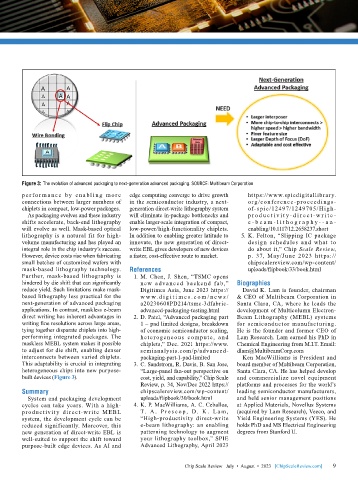
Figure 3: The evolution of advanced packaging to next-generation advanced packaging. SOURCE: Multibeam Corporation
        p e r fo r m a n c e b y e n a bl i ng m o r e   edge computing converge to drive growth   https://www.spiedigitallibrary.
        connections between larger numbers of   in the semiconductor industry, a next-  org /con ference -proceed i ngs-
        chiplets in compact, low-power packages.  generation direct-write lithography system   of-spie/12497/1249705/ Hig h-
          As packaging evolves and these industry   will eliminate in-package bottlenecks and   p r o d u c t iv i t y - d i r e c t - w r i t e -
        shifts accelerate, back-end lithography   enable larger-scale integration of compact,   e - b e a m -l it h og r a p hy - - a n -
        will evolve as well. Mask-based optical   low-power/high-functionality chiplets.   enabling/10.1117/12.2658237.short
        lithography is a natural fit for high-  In addition to enabling greater latitude to   5.  K. Felton, “Slipping IC package
        volume manufacturing and has played an   innovate, the new generation of direct-  design  schedules  and  what  to
        integral role in the chip industry’s success.   write EBL gives developers of new devices   do about it,” Chip Scale Review,
        However, device costs rise when fabricating   a faster, cost-effective route to market.  p. 37, May/June 2023 https://
        small batches of customized wafers with                                   chipscalereview.com/wp-content/
        mask-based lithography technology.   References                           uploads/flipbook/33/book.html
        Further, mask-based lithography is   1.  M. Chen, J. Shen, “TSMC opens
        hindered by die shift that can significantly   new a dva nced backend fab,”   Biographies
        reduce yield. Such limitations make mask-  Digitimes Asia, June 2023 https://  David K. Lam is founder, chairman
        based lithography less practical for the   w w w. d i g i t i me s . c om / ne ws /  & CEO of Multibeam Corporation in
        next-generation of advanced packaging   a20230608PD214/tsmc-3dfabric-  Santa Clara, CA, where he leads the
        applications. In contrast, maskless e-beam   advanced-packaging-testing.html  development of Multicolumn Electron-
        direct writing has inherent advantages in   2.  D. Patel, “Advanced packaging part   Beam Lithography (MEBL) systems
        writing fine resolutions across large areas,   1 – pad limited designs, breakdown   for semiconductor manufacturing.
        tying together disparate chiplets into high-  of economic semiconductor scaling,   He is the founder and former CEO of
        performing integrated packages. The    het e rogeneou s comput e, a nd   Lam Research. Lam earned his PhD in
        maskless MEBL system makes it possible   chiplets,” Dec. 2021 https://www.  Chemical Engineering from M.I.T. Email:
        to adjust for die shift, enabling denser   semianalysis.com/p/advanced-  dlam@MultibeamCorp.com
        interconnects between varied chiplets.   packaging-part-1-pad-limited   Ken MacWilliams is President and
        This adaptability is crucial in integrating   3.  C. Sandstrom, R. Davis, B. San Jose,   board member of Multibeam Corporation,
        heterogeneous chips into new purpose-  “Large-panel fan-out perspective on   Santa Clara, CA. He has helped develop
        built devices (Figure 3).              cost, yield, and capability,” Chip Scale   and commercialize novel equipment
                                               Review, p. 34, Nov/Dec 2022 https://  platforms and processes for the world’s
        Summary                                chipscalereview.com/wp-content/  leading semiconductor manufacturers,
          System and packaging development     uploads/flipbook/30/book.html  and held senior management positions
        cycles can take years. With a high-  4.  K. P. MacWilliams, A. C. Ceballos,   at Applied Materials, Novellus Systems
        product ivit y d i rect-w r ite M EBL   T. A . P r e s c o p , D. K . L a m ,   (acquired by Lam Research), Veeco, and
        system, the development cycle can be   “High-productivity direct-write   Yield Engineering Systems (YES). He
        reduced significantly. Moreover, this   e-beam lithography: an enabling   holds PhD and MS Electrical Engineering
        new generation of direct-write EBL is   patterning technology to augment   degrees from Stanford U.
        well-suited to support the shift toward   your lithography toolbox,” SPIE
        purpose-built edge devices. As AI and   Advanced Lithography, April 2023


                                                             Chip Scale Review   July  •  August  •  2023   [ChipScaleReview.com]  9 9