
Page 21 - Chip Scale Review_July August_2023-digital
P. 21
Heterogeneous integration of chiplets technology enabled
by advanced package architectures, first-level interconnect
By Nelson Fan, Eric Ng [ASMPT Limited]
W hile leading semiconductor effects of expensive nodes. To achieve Various HI package architectures
companies continue to
degree of chiplets placement accuracy
develop complementary the required performance, a very high Over the last decade, various HI package
architectures have been developed by
metal-oxide semiconductor (CMOS) in a heterogeneously-integrated (HI) the technology frontrunners including
scaling under the driving forces of high- device is being scaled up, and more wafer foundries, integrated device
performance computing (HPC) and artificial advanced FLI interconnect processes are manufacturers (IDMs), outsourced
intelligence (AI) applications, “More than being developed. From traditional mass semiconductor assembly and test
Moore” has been successfully demonstrated reflow flip chip (MR-FC) and thermal suppliers (OSATs), and advanced
through the heterogeneous integration of compression bonding (TCB) at 5µm and substrate houses (Figure 2). These HI
chiplets (HIC) in various advanced package 2µm placement accuracy respectively, package architectures can be classified
architectures, together with advanced the technology is now evolving towards into three major basic categories: 1) with
first-level interconnect (FLI) technologies fluxless thermal compression bonding a through-silicon via (TSV) interposer;
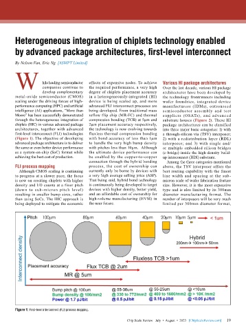
(Figure 1). The objective of developing with bond accuracy of less than 1µm 2) with a redistribution layer (RDL)
advanced package architecture is to deliver to handle the very high bump density interposer; and 3) with single and/
the same or even better device performance with pitches less than 10µm. Although or multiple embedded silicon bridges
as a system-on-chip (SoC) format while the ultimate device performance can (e-bridge) inside the high-density build-
achieving the best cost of production. be enabled by the copper-to-copper up interconnect (HDI) substrate.
connection through the hybrid bonding Among the three categories mentioned
FLI process mapping process, the cost of ownership can above, the TSV interposer offers the
Although CMOS scaling is continuing currently only be borne by devices with best routing capability with the finest
to progress at a slower pace, the focus a very high average selling price (ASP). line width and spacing at the sub-
is now on creating chiplets with higher That being said, hybrid bond technology micron scale of wafer fabrication feature
density and I/O counts at a finer pitch is continuously being developed to target size. However, it is the most expensive
(down to sub-micron pitch level) devices with higher density, better yield, type and is also limited by its 300mm
resulting in smaller bump sizes, rather and an affordable cost of ownership for diameter manufacturing format. The
than using SoCs. The HIC approach is high-volume manufacturing (HVM) in number of interposers will be very much
being deployed to mitigate the economic the near future. limited per 300mm diameter format,
Figure 1: First-level interconnect (FLI) process mapping.
19
Chip Scale Review July • August • 2023 [ChipScaleReview.com] 19