
Page 28 - Chip Scale Review_July August_2023-digital
P. 28
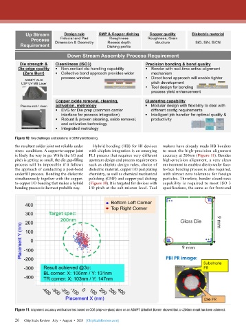
Figure 10: Key challenges and solutions in D2W hybrid bonding.
        the resultant solder joint not reliable under   Hybrid bonding (HB) for HI devices   makers have already made HB bonders
        stress  conditions. A copper-to-copper joint   with chiplets integration is an emerging   to meet the high-precision alignment
        is likely the way to go. While the I/O pad   FLI process that requires very different   accuracy at 200nm (Figure 11). Besides
        pitch is getting so small, the die gap-filling   upstream design and process requirements   high-precision alignment, a very clean
        process will be impossible if it follows   such as chiplets design rules, choice of   environment to enable a die-to-wafer face-
        the approach of conducting a post-bond   dielectric material, copper I/O pad plating   to-face bonding process is also required,
        underfill process. Bonding the dielectric   chemistry, as well as chemical mechanical   with almost zero tolerance for foreign
        simultaneously together with the copper-  polishing (CMP) and copper pad dishing    particles. Therefore, bonder cleanliness
        to-copper I/O bonding that makes a hybrid   (Figure 10). It is targeted for devices with   capability is required to meet ISO 3
        bonding process is the most probable way.  I/O pitch at the sub-micron level. Tool   specifications, the same as for front-end


        Figure 11: Alignment accuracy verification test based on COG (chip-on-glass) done on an ASMPT LithoBolt Bonder showed that a ≤200nm result has been achieved.

        26
        26   Chip Scale Review   July  •  August  •  2023   [ChipScaleReview.com]