Page 22 - Chip Scale Review_Jul Aug_2022-digital
P. 22
to micron length, along with high area
                                                                              interconnect densities enabled by finer
                                                                              pitches, enables a true 3D structure
                                                                              with reduced footprint, low latency and
                                                                              high bandwidth while increasing the
                                                                              total SoC area. In addition to packaging
                                                                              portioned SoC dies, hybrid bonding
                                                                              enables st ack i ng of 3D dy namic
                                                                              random access memor y (DR AM),
                                                                              heterogeneous integration at high I/O
                                                                              densities, lower power consumption,
                                                                              and form factor reduction.

                                                                              CPO
                                                                                The next level of per for mance
                                                                              packaging for long-distance signal
                                                                              t ransmission is moving f rom the
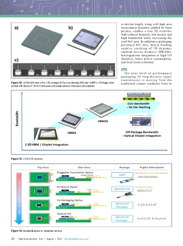
        Figure 12: a) BGA side view of the 2.5D package; b) Top view showing ASIC and 4 HBM’s; c) Package cross-  traditional copper conductor lines to
        section with details of TSV in Si interposer and bumps between interposer and substrate.


        Figure 13: 2.5D to 3D evolution.


        Figure 14: Bandwidth/power vs. integration method.

        20   Chip Scale Review   July  •  August  •  2022   [ChipScaleReview.com]
        20

