Page 17 - Chip Scale Review_Jul Aug_2022-digital
P. 17
dies). The FOCoS-B package body size is
                                                                                      2
                                                                              78x70mm  with two fan-out chip modules
                                                                              at a size of 47x31mm , respectively.
                                                                                                  2
                                                                              FOCoS-B packages have passed reliability
                                                                              tests and chiplets integration has achieved
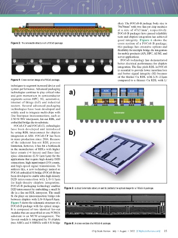
                                                                              good integrity.  Figure 6 shows the
        Figure 3: The schematic structure of a FOCoS package.                 cross-section of a FOCoS-B package;
                                                                              this package has extensive options and
                                                                              flexibility for multiple bridge die integration
                                                                              for mobile products (AP), HPC, AI/ML and
                                                                              server applications.
                                                                                FOCoS technology has demonstrated
                                                                              better electrical performance for chiplets
                                                                              integration. The fine-pitch RDL in FOCoS
                                                                              is essential to provide lower insertion loss
                                                                              and better signal integrity (SI) because
                                                                              of the thicker Cu RDL with L/S=2/2µm
        Figure 4: Cross-section image of a FOCoS package.                     compared to a thinner Cu RDL with L/
        techniques to augment increased device and
        system performance. Advanced packaging
        technologies continue to play critical roles
        and gain momentum in semiconductor
        segments across HPC, 5G, automotive,
        internet of things (IoT) and industrial
        sectors. Several advanced packaging
        technologies have been developed and
        widely used to integrate multi-chips with
        fine line/space interconnections, such as
        2.5D Si TSV interposers, fan-out RDL, and
        embedded bridge die-in-substrate.
          FOCoS-CF and FOCoS-CL technologies
        have been developed and introduced
        by using RDL interconnect for chiplets
        integration at ASE. FOCoS-CF has been
        in mass production since 2016. Because
        of the inherent fan-out RDL process
        limitation, however, it has hit a bottleneck
        in the manufacture of RDLs with higher
        layer counts (>6 layers) and finer line/
        space dimensions (L/S<1µm/1µm) for the
        applications that require high-density D2D
        connections, high input/output (I/O) counts,
        and high-speed signal transmission. To
        address this, a new technology named as
        FOCoS embedded Si bridge (FOCoS-B) has
        been developed to enable ultra-high density
        D2D interconnection with L/S<1/1µm
        for high-density chiplets integration.
        FOCoS-B packaging technology enables
        D2D interconnect by embedding a small Si   Figure 5: a) (top) Schematic structure and b) (bottom) the optical image for a FOCoS-B package.
        die in a fan out RDL interposer. The small
        Si die plays an interconnection bridge role
        between chiplets with L/S<0.8µm/0.8µm.
        Figure 5 shows the schematic structure of a
        FOCoS-B package with the optical image.
        It is composed of two identical fan-out
        modules that are assembled on one FCBGA
        substrate in an MCM arrangement. The
        fan-out module is integrated by 10 chiplets
        (two ASICs and 8 HBM2e with 8 Si bridge   Figure 6: A cross-section of a FOCoS-B package.

                                                                                                             15
                                                             Chip Scale Review   July  •  August  •  2022   [ChipScaleReview.com]  15

