Page 19 - Chip Scale Review_Jul Aug_2022-digital
P. 19
When we look at the various package
                                                                              platform roadmaps today, we see a trend
                                                                              around miniaturization, not necessarily
                                                                              just for final package size, but also for
                                                                              performance. For the mobile space,
                                                                              the original equipment manufacturer
                                                                              (OEM) suppliers are driving component
                                                                              size reduction or integration across
                                                                              all sub-modules to enable more room
                                                                              for new functionality while managing
                                                                              battery space.
                                                                                Table 1 by TSR in February 2022
                                                                              shows the modular adoption rate
                                                                              across various radio frequency (RF)
                                                                              modules. The one reduced adoption
                                                                              is partially due to the exit of LG,
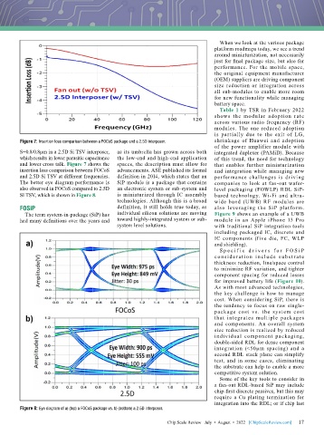
        Figure 7: Insertion loss comparison between a FOCoS package and a 2.5D interposer.  shrinkage of Huawei  and adoption
                                                                              of the power amplifier module with
        S=0.8/0.8µm in a 2.5D Si TSV interposer,   as its umbrella has grown across both   integrated duplexer (PAMiD). Because
        which results in lower parasitic capacitance   the low-end and high-end application   of this trend, the need for technology
        and lower cross talk. Figure 7 shows the   spaces, the description must allow for   that enables further miniaturization
        insertion loss comparison between FOCoS   advancements. ASE published its formal   and integration while managing new
        and 2.5D Si TSV at different frequencies.   definition in 2014, which states that an   performance challenges is driving
        The better eye diagram performance is   SiP module is a package that contains   companies to look at fan-out wafer-
        also observed in FOCoS compared to 2.5D   an electronic system or sub-system and   level packaging (FOWLP) RDL SiP-
        SI TSV, which is shown in Figure 8.  is miniaturized through IC assembly   based technology. Wi-Fi and ultra-
                                           technologies. Although this is a broad   wide band (UWB) RF modules are
        FOSiP                              definition, it still holds true today, as   also leveraging the SiP platform.
          The term system-in-package (SiP) has   individual silicon solutions are moving   Figure 9 shows an example of a UWB
        had many definitions over the years and   toward highly-integrated system or sub-  module  in  an  Apple  iPhone  13  Pro
                                           system level solutions.            with traditional SiP integration tools
                                                                              including packaged IC, discrete and
                                                                              IC components (five die, FC, WLP
                                                                              and shielding).
                                                                                S p e c i f i c d r i v e r s f o r F OS i P
                                                                              c on side r at ion i nclude s ubst r at e
                                                                              thickness reduction, line/space control
                                                                              to minimize RF variation, and tighter
                                                                              component spacing for reduced losses
                                                                              for improved battery life (Figure 10).
                                                                              As with most advanced technologies,
                                                                              the key challenge is how to manage
                                                                              cost. When considering SiP, there is
                                                                              the tendency to focus on raw single-
                                                                              package cost vs. the system cost
                                                                              that integrates multiple packages
                                                                              and components. An overall system
                                                                              size reduction is realized by reduced
                                                                              individual component packaging,
                                                                              double-sided RDL for dense component
                                                                              integration (<50µm spacing) and a
                                                                              second RDL stack plane can simplify
                                                                              test, and in some cases, eliminating
                                                                              the substrate can help to enable a more
                                                                              competitive system solution.
                                                                                Some of the key tools to consider in
                                                                              a fan-out RDL-based SiP may include
                                                                              chip-first discrete passives, but this may
                                                                              require a Cu plating termination for
                                                                              integration into the RDL; or if chip last
        Figure 8: Eye diagram of a) (top) a FOCoS package vs. b) (bottom) a 2.5D interposer.

                                                                                                             17
                                                             Chip Scale Review   July  •  August  •  2022   [ChipScaleReview.com]  17

