Page 20 - Chip Scale Review_Jul Aug_2022-digital
P. 20

is used, a standard solder termination
                                                                              can be used. In addition, integrated or
                                                                              created passive components can also
                                                                              be beneficial. Both 2D and 3D spiral
                                                                              inductors, and even new inductor
                                                                              passives are being developed – within
                                                                              the RDL layers – to further improve
                                                                              the performance allowing them to be
                                                                              integrated and further miniaturized (see
                                                                              Figure 11).

                                                                              2.5D/3D
                                                                                The 2.5D platform with a silicon
                                                                              i nt e r p ose r evolve d a s a n at u r a l
                                                                              progression from MCM on organic
                                                                              substrate because of readily available
                                                                              sub-micron L/S. A 2.5D platform
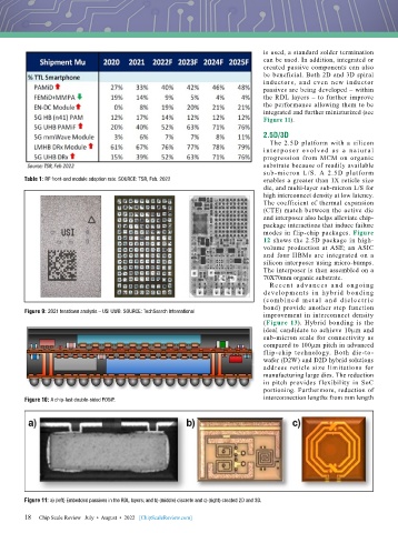
        Table 1: RF front-end module adoption rate. SOURCE: TSR, Feb. 2022    enables a greater than 1X reticle size
                                                                              die, and multi-layer sub-micron L/S for
                                                                              high interconnect density at low latency.
                                                                              The coefficient of thermal expansion
                                                                              (CTE) match between the active die
                                                                              and interposer also helps alleviate chip-
                                                                              package interactions that induce failure
                                                                              modes in flip-chip packages. Figure
                                                                              12 shows the 2.5D package in high-
                                                                              volume production at ASE; an ASIC
                                                                              and four HBMs are integrated on a
                                                                              silicon interposer using micro-bumps.
                                                                              The interposer is then assembled on a
                                                                              70X70mm organic substrate.
                                                                                Re c e nt a dva nc e s a nd ongoi ng
                                                                              developments i n hybr id bondi ng
                                                                              (c ombi ne d me t a l a nd d iele c t r ic
                                                                              bond) provide another step function
        Figure 9: 2021 teardown analysis – USI UWB. SOURCE: TechSearch International
                                                                              improvement in interconnect density
                                                                              (Figure 13). Hybrid bonding is the
                                                                              ideal candidate to achieve 10μm and
                                                                              sub-micron scale for connectivity as
                                                                              compared to 100µm pitch in advanced
                                                                              f lip-chip technology. Both die-to-
                                                                              wafer (D2W) and D2D hybrid solutions
                                                                              address reticle size limitations for
                                                                              manufacturing large dies. The reduction
                                                                              in pitch provides flexibility in SoC
                                                                              portioning. Furthermore, reduction of
        Figure 10: A chip-last double-sided FOSiP.                            interconnection lengths from mm length


        Figure 11: a) (left} Embedded passives in the RDL layers; and b) (middle) discrete and c) (right) created 2D and 3D.

        18
        18   Chip Scale Review   July  •  August  •  2022   [ChipScaleReview.com]
   15   16   17   18   19   20   21   22   23   24   25