Page 15 - Chip Scale Review_Jul Aug_2022-digital
P. 15
Advanced packaging technologies such
                                                                              as flip-chip ball grid array (FCBGA),
                                                                              multi-chip modules (MCMs), and 2.5D
                                                                              Si through-silicon vias (TSVs) have been
                                                                              widely used for chiplets and die-to-die
                                                                              (D2D) interconnections across various
                                                                              semiconductor segments. However, with
                                                                              increasing demands for high density,
                                                                              high speed and low latency of  D2D
                                                                              interconnects, the FC MCM package
                                                                              has reached its limit due to the large Cu
                                                                              interconnect line/space L/S>5/5µm in the
                                                                              substrate, and unsustainable costs related
                                                                              to 2.5D Si TSV with larger interposer size
                                                                              (>2X reticle size). Therefore, alternative
                                                                              packaging solutions such as 2.5D TSV-
                                                                              less and fan-out RDL interposer have
                                                                              been developed in recent years. Three
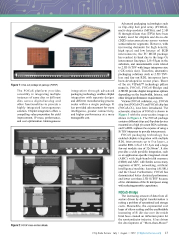
        Figure 1: A fan-out package on package (FOPoP).                       of the six VIPack™ technology pillars
                                                                              namely, FOCoS, FOCoS-Bridge and
            The FOCoS platform provides        integration through advanced   2.5D/3D provide chiplet integration options
            versatility in integrating multiple   packaging technology enables chiplet   depending on the bandwidth, latency, and
            instances of same dies or different   integration with separate designs   other design/performance requirements.
            dies across digital/analog and     and different manufacturing process   Various FOCoS solutions, e.g., FOCoS
            other functionalities to provide a   nodes within a single package. It   chip first (FOCoS-CF) and FOCoS chip last
            highly integrated heterogeneous    has provided advancement for more   (FOCoS-CL), have been introduced. The
            solution. Chiplet integration offers a   intelligence, greater connectivity,   schematic structure of FOCoS is shown in
            compelling value proposition for yield   and higher performance at a more   Figure 3 with the cross-section image as
            improvement, IP reuse, performance,   manageable cost.            shown in Figure 4. The FOCoS package
            and cost optimization. Heterogeneous                              contains different chips and flip-chip devices
                                                                              mounted on a high pin count BGA substrate,
                                                                              and Cu RDL replaces the expense of using a
                                                                              Si TSV interposer to provide interconnects.
                                                                                FOCoS packaging technology has
                                                                              enabled chiplets integration with multiple
                                                                              RDL interconnects up to five layers, a
                                                                              smaller RDL L/S of 1.5/1.5µm and a large
                                                                                                        2
                                                                              fan-out module size of 32x38mm . It also
                                                                              provides a wide portfolio integration, such
                                                                              as an application-specific integrated circuit
                                                                              (ASIC) with high-bandwidth memory
                                                                              (HBM) and ASIC with Serdes across many
                                                                              segments of HPC, networking, artificial
                                                                              intelligence/machine learning (AI/ML)
                                                                              and the Cloud. Furthermore, FOCoS has
                                                                              demonstrated better electrical performance
                                                                              and lower cost than 2.5D Si TSV because
                                                                              of the elimination of the Si interposer along
                                                                              with reducing parasitic capacitance.

                                                                              FOCoS-Bridge
                                                                                The increasing amount of data from all
                                                                              sectors driven by digital transformation is
                                                                              raising a problem of operational and storage
                                                                              costs. Meanwhile, the exponential cost
                                                                              leaps of silicon scaling and the unaffordable
                                                                              increasing of Si die size over the reticle
                                                                              limit have created an inflection point for
                                                                              the semiconductor industry. It has driven
                                                                              the development of “More-than-Moore”
        Figure 2: FOPoP cross-section details.

                                                                                                             13
                                                             Chip Scale Review   July  •  August  •  2022   [ChipScaleReview.com]  13

