Page 12 - Chip Scale Review_Jul Aug_2022-digital
P. 12
Summary
                                                                                Thermal management for wafer
                                                                              test is changing dynamically because
                                                                              of increased parallelism, high-power
                                                                              densities, and complex IC designs. To
                                                                              ensure that a device is tested at the
                                                                              desired temperature, wafer chucks with
                                                                              multiple temperature sensors, as well as
                                                                              liquid-cooled capabilities, are required
                                                                              for timely high-power dissipation.  In
                                                                              addition, smart thermal management
                                                                              solutions are crucial for avoiding burnt
                                                                              probes and damaged devices, to ensure
                                                                              high test cell uptime.  Various customer
                                                                              production case studies have shown
                                                                              the necessities of using a low thermal
                                                                              resistance wafer chuck systems with
                                                                              multiple temperature sensors, including
                                                                              full-wafer contact memory testing with
                                                                              up to 2000W, medium-contact areas with
                                                                              up to 400W, and small-contact areas
                                                                              of a few DUTs with up to 160W. With
                                                                              leading-edge SoCs, high-bandwidth
                                                                              memory testing, and heterogeneous
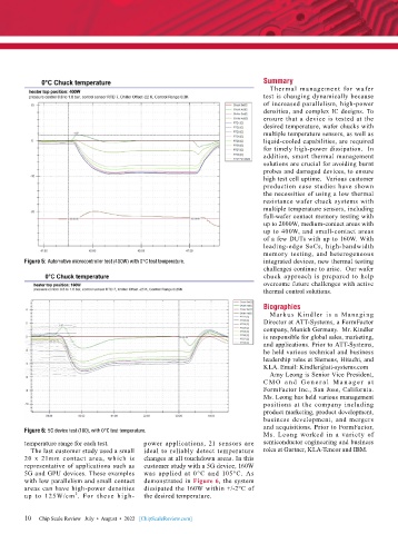
        Figure 5: Automotive microcontroller test (400W) with 0°C test temperature.  integrated devices, new thermal testing
                                                                              challenges continue to arise.  Our wafer
                                                                              chuck approach is prepared to help
                                                                              overcome future challenges with active
                                                                              thermal control solutions.
                                                                              Biographies
                                                                                Mark us Kindler is a Managing
                                                                              Director at ATT-Systems, a FormFactor
                                                                              company, Munich Germany.  Mr. Kindler
                                                                              is responsible for global sales, marketing,
                                                                              and applications. Prior to ATT-Systems,
                                                                              he held various technical and business
                                                                              leadership roles at Siemens, Hitachi, and
                                                                              KLA. Email: Kindler@att-systems.com
                                                                                Amy Leong is Senior Vice President,
                                                                              C M O a n d G e n e r a l M a n a g e r a t
                                                                              FormFactor Inc., San Jose, California.
                                                                              Ms. Leong has held various management
                                                                              positions at the company including
                                                                              product marketing, product development,
                                                                              business development, and mergers
                                                                              and acquisitions. Prior to FormFactor,
        Figure 6: 5G device test (160), with 0°C test temperature.
                                                                              Ms. Leong worked in a variety of
        temperature range for each test.   power applications, 21 sensors are   semiconductor engineering and business
          The last customer study used a small   ideal to reliably detect temperature   roles at Gartner, KLA-Tencor and IBM.
        20 x 21mm contact area, which is   changes at all touchdown areas. In this
        representative of applications such as   customer study with a 5G device, 160W
        5G and GPU devices. These examples   was applied at  0°C and 105°C. As
        with low parallelism and small contact   demonstrated in Figure 6, the system
        areas can have high-power densities   dissipated the 160W within +/-2°C of
        up  to  125W/cm .  For  these  high-  the desired temperature.
                       2

        10   Chip Scale Review   July  •  August  •  2022   [ChipScaleReview.com]
        10

