Page 10 - Chip Scale Review_Jul Aug_2022-digital
P. 10
Detecting the temperature in real time and with accuracy
                                                             are essential first steps to controlling it. ATT-Systems’ low-
                                                             thermal-resistance (LTR) wafer chucks include a MultiSense
                                                             option, which places multiple sensors across the chuck to
                                                             accurately measure the temperature. The number of sensors
                                                             used varies depending on the application, and is mainly
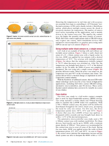
                                                             driven by the contact area size. The smaller the contact
        Figure 2: Number of sensors scaled to contact area size, ordered from low- to   area, the higher the quantity and array density of sensors.
        high-sensor array density.                           While full-wafer contact applications such as DRAM testing
                                                             only  require one sensor, multi-touchdown devices like
                                                             automotive microcontrollers or graphics processing units
                                                             (GPUs) can use up to 21 sensors (Figure 2).

                                                             Using multiple wafer chuck sensors vs. a single sensor
                                                               Let’s look at an example of testing with and without our
                                                             multiple sensor solution. Figure 3 shows a wafer chuck test
                                                             setup of a 21 x 22mm contact area with a liquid cooler. In
                                                             this test, 200W was applied for two minutes with a desired
                                                             temperature of 70°C. The solution with multiple sensors
                                                             (Figure 3a) shows that the temperature initially jumped
                                                             to 74.1°C when the power was switched on. After 28s, the
                                                             temperature was brought back down to +/-1°C of the desired
                                                             number. At the 33s mark, the 200W of power was completely
                                                             dissipated. The test using only a single sensor (Figure 3b)
                                                             presents different results. When the power was turned on, the
                                                             temperature rose past 96°C in the two-minute time frame. The
                                                             system did not detect a thermal change or implement an active
                                                             temperature control solution.
                                                               With the flexibility of additional sensors, this new LTR wafer
                                                             chuck technology can be used for a wide variety of high-power
                                                             applications, including full-wafer contact DRAM testing,
                                                             automotive microcontrollers, and 5G devices. These active
                                                             thermal control solutions have proven to be valuable in a series
                                                             of case studies.
                                                             Case studies
                                                               The first case study is a full-wafer contact example
                                                             that is used for high-bandwidth memory (HBM) testing.
                                                             The  setup  includes  a  wafer  chuck  and  300mm  heating
        Figure 3: a) Multiple sensors vs. b) single-sensor temperature response and   plate to simulate the 2,000W wafer test conditions. With
        control results.                                     a 300 x 300mm contact area, the power will be uniformly
                                                             distributed throughout the entire chuck area, prompting
                                                             the need for only one sensor. For this test, the three
                                                             temperature points were -40°C, 25°C and 125°C. Figure
                                                             4 shows that once the 2,000W of heat was applied, it
                                                             dissipated within seconds and was brought back down to
                                                             within +/-2°C of the desired temperature.
                                                               The automotive microcontroller case study used a 100
                                                             x 100mm contact area with medium parallelism. For these
                                                             devices, heat transfer can be up to 1000W, with a moderate
                                                                                 2
                                                             power density of 10W/cm . Nine sensors are recommended for
                                                             this contact area size to cover all areas of the chuck. During
                                                             the case study, 400W was applied across the wafer at three
                                                             temperature points: 0°C, 85°C and 105°C. As seen in Figure
                                                             5, the correct sensor detected the temperature increase and the
                                                             chuck system was able to dissipate the 400W within a +/-2°C
        Figure 4: Full-wafer contact test (2000W) with -40°C test temperature.

        8 8  Chip Scale Review   July  •  August  •  2022   [ChipScaleReview.com]

