Page 27 - Chip Scale Review_Jul Aug_2022-digital
P. 27
MB signals included some tight signal-  a 50Ω test environment has now been   alignment and connectivity are to be
        ground spacing that would not allow for   implemented on a cViper probe stack-  achieved across all sites.  Customers
        a wider signal probe. Instead, a wider   up and PCB layout and measured after   expect to be able to swap out probe
        ground probe was designed that could   assembly to verify that the targeted   heads locally, without requiring a time-
        be used in selected ground locations to   performance is being achieved.  consuming realignment process.
        reduce the overall impedance of the MB                                  The initial probe head and PCB
        cross section.                     Probe head to probe card alignment   design have evolved in several ways
          A new ground probe was designed   improvements                      to improve the alignment mechanism.
        a n d  b u i lt  t o  m a t c h  s e ve r a l  ke y   When fitting probe heads to probe   Monte Carlo analysis techniques were
        parameters of the original signal probe,   cards for such fine-pitch applications,   used to identify the features of the
        including test height, spring force at test   there is no margin for error if good   design that had the greatest impact on
        height and crown tip profile where the
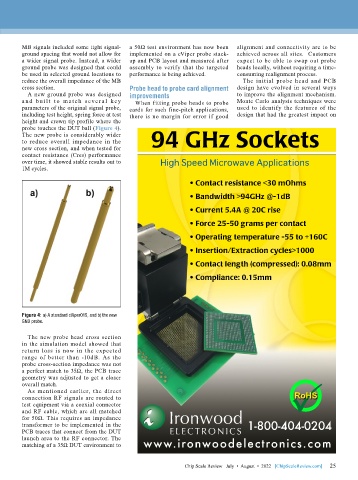
        probe touches the DUT ball (Figure 4).
        The new probe is considerably wider
        to reduce overall impedance in the
        new cross section, and when tested for
        contact resistance (Cres) performance
        over time, it showed stable results out to
        1M cycles.


        Figure 4: a) A standard cViper015, and b) the new
        GND probe.

          The new probe head cross section
        in the simulation model showed that
        return loss is now in the expected
        range of better than -10dB. As the
        probe cross-section impedance was not
        a perfect match to 35Ω, the PCB trace
        geometry was adjusted to get a closer
        overall match.
          As mentioned earlier, the direct
                                                                                                 RoHS
        connection RF signals are routed to                                                     P
        test equipment via a coaxial connector
        and RF cable, which are all matched
        for 50Ω. This requires an impedance
        transformer to be implemented in the
        PCB traces that connect from the DUT
        launch area to the RF connector. The
        matching of a 35Ω DUT environment to


                                                                                                             25
                                                             Chip Scale Review   July  •  August  •  2022   [ChipScaleReview.com]  25

