Page 29 - Chip Scale Review_Jul Aug_2022-digital
P. 29
validation to be performed on a complete
                                                                              probe head + PCB assembly, using a probe
                                                                              card analyzer. A design of experiments
                                                                              (DOE) has been defined to assess the
                                                                              variability of the manufacturing processes,
                                                                              using several copies of the probe heads and
                                                                              PCBs, which are manufactured at different
                                                                              times and will be assembled and tested in
                                                                              different combinations.
                                                                              More efficient multi-site layout
                                                                                For high-volume production test, a more
                                                                              compact multi-site layout is preferred, as
                                                                              it will typically result in fewer skipped die
                                                                              when testing near the edge of the wafer,
                                                                              thereby translating into higher overall
                                                                              touchdown efficiency, higher throughput,
                                                                              and therefore, a lower cost of test (COT).
                                                                              The original test site layout implemented 8
                                                                              sites in a 1x8 single row, with three skipped
                                                                              die between each site. This was required to
                                                                              accommodate the large amount of RF test
                                                                              circuitry routed out from each site.
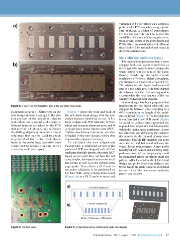
                                                                                A new design has been proposed that
        Figure 5: a) (top) Front and b) (bottom) back of the new probe head design.  implements the 1x8 layout with only one
                                                                              skipped die between sites, resulting in a
        alignment accuracy. Differences in the   Figure 5 shows the front and back of   48% reduction in the length of the multi-
        new design include a change to the size   the new probe head design with the new   site test layout (Figure 7). The first step was
        and position of the alignment pins to   design features identified in red: 1) Six   to confirm that a new PCB layout (Figure
        make them more robust and accurate.   holes to align with PCB fiducials; 2) More   8) could be defined that supported the
        Fiducial features are added on the PCB   robust and accurate alignment pins; and 3)   required level of per-site test functionality
        that provide a high-accuracy reference   A single-piece probe retainer plate (PRP).   within the tighter space restrictions. A new
        for drilling alignment holes and a visual   Tighter machining tolerances are also   test schematic was defined by the customer
        reference that can be used to check   included in the new design, where this   that allowed for the removal of some trace
        alignment of the probe head. Some   improves the alignment accuracy.   structures. Specific RF insertion loss goals
        items in the probe head assembly were   To  validate  the  new alig n ment   were also defined that would influence the
        simplified to reduce stack-up errors   mechanisms, a simplified version of the   overall layout requirements. A new probe
        across the multi-site layout.      probe card PCB was designed and built that   head layout was defined and a bowing study
                                           duplicates the high-density, fine-pitch DUT   performed to confirm that planarity could
                                           layout across eight sites, but fans this out   be maintained across the denser multi-site
                                           using simpler, low-speed traces to electrical   pattern. After the constraints of the circuit
                                           test points, as well as to the normal tester   design and probe head were defined, the
                                           pogo pads. This allows a DUT-pad to   layout feasibility study could be completed
                                           test point validation to be performed on   to confirm that the new, denser multi-site
                                           the bare PCB, using a flying probe tester   pattern was possible.
                                           (Figure 6), or a DUT probe to tester pad


        Figure 6: Test PCB layout.         Figure 7: a) (top) Before and b) (bottom) after probe head layouts.

                                                                                                             27
                                                             Chip Scale Review   July  •  August  •  2022   [ChipScaleReview.com]  27

