Page 30 - Chip Scale Review_Jul Aug_2022-digital
P. 30
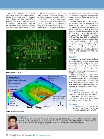
The bowing analysis used ANSYS   of the test area would exceed a target   was also extended between each site area
        simulation tools to model the stresses   limit of 50μm. To reduce bowing, the   and with these changes, the bowing within
        created by the 8 x 600 probes in the probe   attachment points for the probe head were   the DUT area was reduced to less than the
        head design. The design uses a one-  moved closer to the DUT area (Figure   50μm threshold.
        piece ceramic body to house the probes,   9). This creates additional challenges   Initial feasibility studies for the denser
        surrounded by a stainless-steel frame, but   for the PCB routing, so it is important to   8-site layout confirm it is possible to
        even with this, the initial analysis indicated   define the two designs in parallel to avoid   include all the required RF functionality
        that maximum deformation in the center   surprises later! The stainless-steel frame   and manage the increased bowing stresses
                                                                              on the probe head. Follow-on work can
                                                                              include a complete routing and fabrication
                                                                              of the new design, but the possibility
                                                                              to create a 16-site pattern is also being
                                                                              explored. The final design would need
                                                                              to accommodate all the signal routing
                                                                              requirements and respect the layout
                                                                              restrictions created by the probe head
                                                                              attachment and alignment features. The
                                                                              RF cabling used is being reviewed, to see
                                                                              if shorter lengths will be usable in the new
                                                                              layout to help minimize insertion loss
                                                                              contribution.

                                                                              Summary
                                                                                A complex probe card design has been
                                                                              deployed at multiple customer locations and
                                                                              successfully used for validation and test of
                                                                              new mmWave transducers. Because nothing
                                                                              stands still in our technology-driven world,
                                                                              the design has evolved in several areas to
                                                                              meet new customer requirements, improve
        Figure 8: New PCB layout.                                             usability and reduce COT.
                                                                                Mu lt iple de sig n cha nge s we re
                                                                              implemented to match 35Ω impedance
                                                                              of the mmWave MB signals and improve
                                                                              alignment of the probe head and probe card
                                                                              PCB. Options to increase the density of the
                                                                              multi-site test pattern have been validated for
                                                                              feasibility and development has been started.

                                                                              Acknowledgements
                                                                                The author thanks the project teams
                                                                              across Cohu and Synergie-CAD for their
                                                                              extensive contributions to this project.
                                                                              This article is based on a presentation
                                                                              originally given at SWTest 2022.
                                                                              Reference
                                                                                1.  J. Mroczkowski, “55GHz octal-
                                                                                   site wafer test probe card for 5G
                                                                                   mmWave devices,” SWTest, 2021.
        Figure 9: Bowing study results.

                       Biography
                         Peter Cockburn is a Senior Product Marketing Manager at Cohu, Inc., Verwood, UK. He received a BSc
                       from the U. of Southampton in UK. He has over 30 years of experience in the ATE industry, including software
                       development, product marketing and program management. Email: peter.cockburn@cohu.com


        28   Chip Scale Review   July  •  August  •  2022   [ChipScaleReview.com]
        28

