Page 18 - Chip Scale Review_May June_2022-digital
P. 18
AMD elevated fan-out bridge        AMD 3DVCache™                      the flexibility to have the CPU die with a
        architecture                         As computer architects know well, large   smaller cache as a standalone product to
          To illustrate the result of one of these   on-die L3 caches can provide instructions   address different markets.
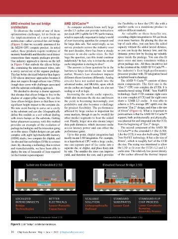
        optimization challenges, let us focus on   per clock (IPC) uplifts for CPU performance,    As valuable as these benefits are,
        the implementation of a new package   which is especially important in today’s world   extending chiplet integration to 3D can break
        architecture called elevated fan-out bridge   of ever-increasing appetites for compute and   even more barriers. By placing the dies on
        (Figure 5) that we recently announced for   for large data sets. Not surprisingly, as we   top of each other, you can have the added
        the MI200 GPU compute product. As noted   survey products across the industry over   capacity without the added lateral distance,
        earlier, these products require terabytes of   the past decades, there has been a steady   so you can keep the latency low, and the
        memory bandwidth and therefore need denser   increase in on-die cache sizes. So that   dynamic power low by freeing up valuable
        connections than organic packages provide.   begs the question, can this trend continue   space inside the package. You can also fit
        One industry approach is shown on the left   indefinitely? In fact, why is it that the on-die   more cores and more transistors within a
        in Figure 5 that embeds the silicon bridge   cache integration is starting to slow?  given package size. All these incentives led
        die, containing the interconnect wires, into   The answers to these questions lie in the   to the creation of the AMD 3D V-Cache™—
        a cavity carved out of the organic package.   barriers to large on-die caches. As noted   the industry’s first high-performance
        This has better electrical behavior than legacy   earlier, Moore’s Law slowdown impacts   processor product with 3D integration based
        2.5D silicon interposer approaches because it   different silicon functions differently. Analog   on hybrid bond technology.
        does not require through-silicon vias (TSVs)   circuits have not scaled much into the   The AMD V-Cache™ consists of three
        though does come with challenges associated   advanced nodes, and SRAMs, upon which   main components. The first one is the
        with the substrate embedding approach.  on-die caches are largely based, are also not   “Zen 3” CPU core complex die (CCD). It is
          We decided to develop a cleaner approach   scaling as well as logic.  manufactured using TSMC 7nm FinFET
        that elevates that silicon bridge to live in the   Increasing the on-die cache capacity,   technology. Each CCD contains eight cores
        shadow of copper pillar bumps. We can thin   which also increases the die size and lowers   in a core complex (CCX) and the eight cores
        these silicon bridges down so that there is no   the yield, is becoming increasingly cost   share a 32MB L3 cache.  It was able to
        significant height impact to the compute die.   prohibitive and also becomes a challenge   achieve a 19% average IPC uplift over the
        We now avoid having to carve out a cavity   for product flexibility. The performance   previous “Zen 2” design, and it has a die size
                                                                                     2
        in the substrate and can also lithographically   afforded by large caches is important for   of 81mm  (Figure 6). What is important to
        define this module as a unit without dealing   some markets, though it can be overkill for   point out here is that the AMD 3D V-Cache™
        with micro bumps on the substrate. Getting   other market segments to bear the added   support, both architecturally and physically,
        better placement accuracy with this method   cost. Finally, larger area also means longer   was planned for and integrated into the CCD,
        provides an example of the evolution of   data path distances, which increases cache   from the beginning of “Zen 3” design.
        package technologies and the innovation going   access latency power and can offset the   The second component of the AMD 3D
        on in this space. Chiplet designs can get quite   performance gains.  V-Cache™ is the extended L3 Die (L3D).
        complex with eight high-bandwidth memory   Up to this point, chiplet integration had   Like the CCD, it was also built using TSMC
        (HBM) stacks, two compute die chiplets, and   mostly meant 2.5D integration. For example,   7nm FinFET technology. It has a die size of
                                                                                   2
        the elevated fan-out bridges (EFBs) to connect   in a hypothetical CPU with a large cache,   41mm , which is roughly half of the CCD
        them. By choosing a technology that is robust   one can separate part of the cache into a   die size. The sizing was intentional to allow
        and manufacturable, we have been able to   separate die, or chiplet, and place them side   the L3D to fit over the CCD’s L2 and L3
        deploy the tens of thousands of these required   by side. The smaller die sizes can improve   cache area. The relatively low power density
        for the Frontier supercomputer.    yield, and therefore the cost, and it provides   of the caches allowed the thermal impact


        Figure 5: 2.5D “bridge” architecture landscape.

        16   Chip Scale Review   May  •  June  •  2022   [ChipScaleReview.com]
        16

