Page 20 - Chip Scale Review_May June_2022-digital
P. 20
both RVDD and VDDM are delivered to the
                                                                              L3D through power TSVs. To better convey
                                                                              the power delivery RDL, the construction in
                                                                              Figure 11 is flipped upside down with the top
                                                                              L3D die on the bottom. RVDD supplies the
                                                                              logic portion of the L3D die, while VDDM
                                                                              powers the SRAM bit cells. The power TSVs
                                                                              are primarily placed in the channels between
                                                                              the SRAM macros in the CCD.
                                                                                The SRAM arrays on the L3D die consist
                                                                              of 512 128KB data macros, and 1088 6KB
                                                                              tag and the (LRU) macros located near the
                                                                              signal TSV columns. It is a dual-rail design
                                                                              using VDDM for the SRAM bitcells and
                                                                              RVDD for the peripheral circuits. As added
                                                                              power can negatively impact performance
                                                                              in a power constrained environment, the
                                                                              L3D arrays are optimized not only for high
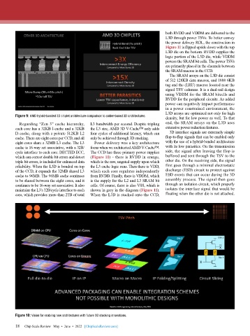
        Figure 9: AMD hybrid-bonded 3D chiplet architecture comparison to solder-based 3D architectures.  density, but for low power as well. To that
          Regarding “Zen 3” cache hierarchy,   L3 bandwidth per second. Despite tripling   end, the SRAM arrays on the L3D uses
        each core has a 32KB I-cache and a 32KB   the L3 size, AMD 3D V-Cache™ only adds   extensive power reduction features.
        D-cache, along with a private 512KB L2   four cycles of additional latency, which can   3D interface signals are extremely simple
        cache. There are eight cores per CCD, and all   only be achieved through 3D stacking.  flop-to-flop signals that can be enabled only
        eight cores share a 32MB L3 cache. The L3   Power delivery was a key architecture   with the use of a hybrid-bonded architecture
        cache is 16-way set associative, with a 32B/  focus when we architected AMD V-Cache™.   with its low parasitics. On the transmission
        cycle interface to each core. DECTED ECC,   The CCD has three primary power supplies   side, the signal after leaving the flop is
        which can correct double bit errors and detect   (Figure 11) – there is RVDD in orange,   buffered and sent through the TSV to the
        triple bit errors, is included for enhanced data   which is the raw, ungated supply upon which   other die. On the receiving side, the signal
        reliability. When the L3D is bonded on top   the L3 cache logic runs. Then there is VDD,   first goes through a minimal electrostatic
        of the CCD, it expands the 32MB shared L3   which each core regulates independently   discharge (ESD) circuit to protect against
        cache to 96MB. The 96MB cache continues   from RVDD. Finally, there is VDDM, which   ESD events that can occur during the 3D
        to be shared between the eight cores, and it   is the supply for the L2 and L3 SRAM bit   assembly process. The signal then goes
        continues to be 16-way set associative. It also   cells. Of course, there is also VSS, which is   through an isolation circuit, which properly
        maintains the L3’s 32B/cycle interface to each   shown in grey in the diagram (Figure 11).   isolates the interface signal that would be
        core, which provides more than 2TB of total   When the L3D is stacked onto the CCD,   floating when the other die is not attached.


        Figure 10: Vision for enabling new architectures with future 3D stacking innovations.

        18   Chip Scale Review   May  •  June  •  2022   [ChipScaleReview.com]
        18

