Page 19 - Chip Scale Review_May June_2022-digital
P. 19
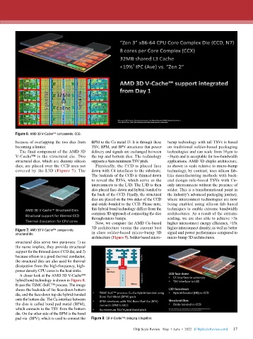
Figure 6: AMD 3D V-Cache™ components: CCD.
        because of overlapping the two dies from   BPM to the Cu metal 13. It is through these   bump technology with tall TSVs is based
        becoming a limiter.                TSV, BPM, and BPV structures that power   on traditional solder-based packaging
          The final component of the AMD 3D   delivery and signals are exchanged between   technologies and can scale from 50μm to
        V-Cache™ is the structural die. Two   the top and bottom dies. The technology   ~36μm and is acceptable for low-bandwidth
        structural dies, which are dummy silicon   supports a 9μm minimum TSV pitch.  applications. AMD 3D chiplet architecture,
        dies, are placed over the CCD area not   Physically, the CCD is placed face   as shown to scale relative to micro-bump
        covered by the L3D (Figure 7). The   down with C4 interfaces to the substrate.   technology, by contrast, uses silicon fab-
                                           The backside of the CCD is thinned down   like manufacturing methods with back-
                                           to reveal the TSVs, which serve as the   end design rule-based TSVs with Cu-
                                           interconnects to the L3D. The L3D is then   only interconnects without the presence of
                                           also placed face-down and hybrid-bonded to   solder. This is a transformational point in
                                           the back of the CCD. Finally, the structural   the industry’s advanced packaging journey,
                                           dies are placed on the two sides of the CCD   where interconnect technologies are now
                                           and oxide-bonded to the CCD. Please note,   being enabled using silicon fab-based
                                           this hybrid bond technology differs from the   techniques to enable extreme bandwidth
                                           common 3D approach of connecting the dies   architectures. As a result of the extreme
                                           through micro-bumps.               scaling, we are also able to achieve >3x
                                             Now, we compare the AMD Cu-based   higher interconnect energy efficiency, >15x
                                           3D architecture versus the current best   higher interconnect density, as well as better
        Figure 7: AMD 3D V-Cache™ components:
        structural die.                    in class solder-based micro-bump 3D   signal and power performance compared to
                                           architecture (Figure 9). Solder-based micro-  micro-bump 3D architectures.
        structural dies serve two purposes: 1) as
        the name implies, they provide structural
        support for the thinned down CCD die; and 2)
        because silicon is a good thermal conductor,
        the structural dies are also used for thermal
        dissipation from the high-frequency, high-
        power density CPU cores to the heat sinks.
          A closer look at the AMD 3D V-Cache™
        hybrid bond technology is shown in Figure 8.
        It uses the TSMC-SoIC™ process. The image
        shows the backside of the face-down bottom
        die, and the face-down top die hybrid-bonded
        onto the bottom die. The Cu interface between
        the dies is called bond pad metal (BPM),
        which connects to the TSV from the bottom
        die. On the other side of the BPM is the bond
        pad via  (BPV), which is used to connect the   Figure 8: 3D V-Cache™: bringing it together.

                                                                                                             17
                                                               Chip Scale Review   May  •  June  •  2022   [ChipScaleReview.com]  17

