Page 14 - Chip Scale Review_May June_2022-digital
P. 14
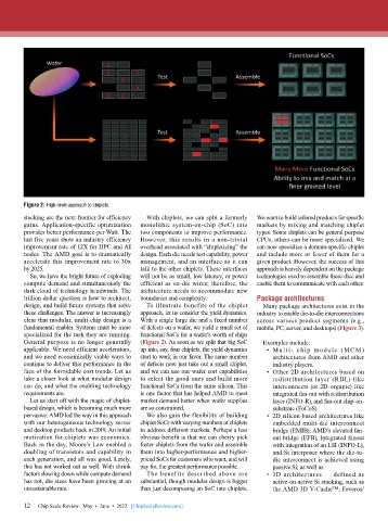
Figure 2: High-level approach to chiplets.
        stacking are the next frontier for efficiency   With chiplets, we can split a formerly   We want to build tailored products for specific
        gains. Application-specific optimization   monolithic system-on-chip (SoC) into   markets by mixing and matching chiplet
        provides better performance-per-Watt. The   two components to improve performance.   types. Some chiplets can be general purpose
        last five years show an industry efficiency   However, this results in a non-trivial   CPUs, others can be more specialized. We
        improvement rate of 12X for HPC and AI   overhead associated with “chipletizing” the   can now specialize a domain-specific chiplet
        nodes. The AMD goal is to dramatically   design. Each die needs test capability, power   and include more or fewer of them for a
        accelerate this improvement rate to 30x    management, and an interface so it can   given product. However, the success of this
        by 2025.                           talk to the other chiplets. These interfaces   approach is heavily dependent on the package
          So, we have the bright future of exploding   will not be as small, low latency, or power   technologies used to assemble these dice and
        compute demand and simultaneously the   efficient as on-die wires; therefore, the   enable them to communicate with each other.
        dark cloud of technology headwinds. The   architecture needs to accommodate new
        trillion-dollar question is how to architect,   boundaries and complexity.  Package architectures
        design, and build future systems that solve   To illustrate benefits of the chiplet   Many package architectures exist in the
        these challenges. The answer is increasingly   approach, let us consider the yield dynamics.   industry to enable die-to-die interconnections
        clear that modular, multi-chip design is a   With a single large die and a fixed number   across various product segments (e.g.,
        fundamental enabler. Systems must be more   of defects on a wafer, we yield a small set of   mobile, PC, server, and desktops) (Figure 3).
        specialized for the task they are running.   functional SoCs for a wafer’s worth of chips
        General purpose is no longer generally   (Figure 2). As soon as we split that big SoC   Examples include:
        applicable. We need efficient accelerators,   up into, say, four chiplets, the yield dynamics   •  Mult i- ch ip module ( MCM )
        and we need economically viable ways to   start to work in our favor. The same number   architectures from AMD and other
        continue to deliver this performance in the   of defects now just take out a small chiplet,   industry players.
        face of the formidable cost trends. Let us   and we can use our wafer sort capabilities   •  Other 2D architectures based on
        take a closer look at what modular design   to select the good ones and build more   redistribution layer (RDL)-like
        can do, and what the enabling technology   functional SoCs from the same silicon. This   interconnects (or 2D-organic) like
        requirements are.                  is one factor that has helped AMD to meet   integrated fan-out with redistribution
          Let us start off with the magic of chiplet-  market demand better when wafer supplies   layer (INFO-R), and fan-out chip-on-
        based design, which is becoming much more   are so constrained.            substrate (FoCoS).
        pervasive. AMD led the way in this approach   We also gain the flexibility of building   •  2D silicon-based architectures like
        with our heterogeneous technology server   chiplet SoCs with varying numbers of chiplets   embedded multi-die interconnect
        and desktop products back in 2019. An initial   to address different markets. Perhaps a less   bridge (EMIB), AMD’s elevated fan-
        motivation for chiplets was economics.   obvious benefit is that we can cherry pick   out bridge (EFB), Integrated fanout
        Back in the day, Moore’s Law enabled a   faster chiplets from the wafer and assemble   with integration of an LSI (INFO-L),
        doubling of transistors and capability in   them into higher-performance and higher-  and Si interposer where the die-to-
        each generation, and all was good. Lately,   priced SoCs for customers who want, and will   die interconnect is achieved using
        this has not worked out as well. With shrink   pay for, the greatest performance possible.  passive Si; as well as
        factors slowing down while compute demand   The  benefits  described  above  are   •  3D architectures — defined as
        has not, die sizes have been growing at an   substantial, though modular design is bigger   active-on-active Si stacking, such as
        unsustainable rate.                than just decomposing an SoC into chiplets.   the AMD 3D V-Cache™, Foveros/

        12   Chip Scale Review   May  •  June  •  2022   [ChipScaleReview.com]
        12

